November 29, 2023
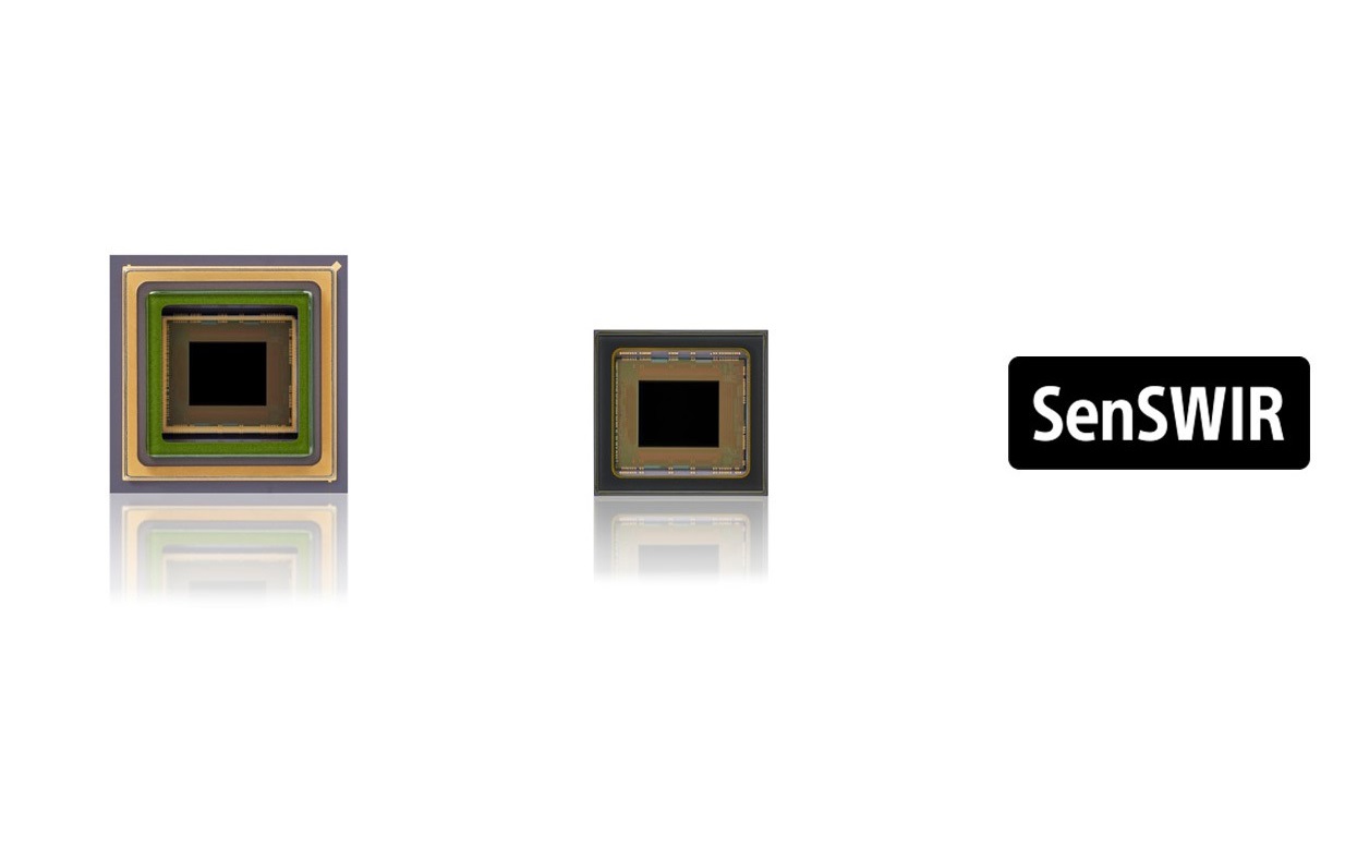
Atsugi, Japan — Sony Semiconductor Solutions Corporation (SSS) today announced the upcoming release of the IMX992 short-wavelength infrared (SWIR) image sensor for industrial equipment, with the industry’s highest pixel count, at 5.32 effective megapixels.
The new sensor uses SSS’s proprietary Cu-Cu connection to achieve the industry’s smallest pixel size of 3.45 μm among SWIR image sensors. It also features an optimized pixel structure for efficiently capturing light, enabling high-definition imaging across a broad spectrum ranging from the visible to invisible short-wavelength infrared regions (wavelength: 0.4 to 1.7 μm). Furthermore, new shooting modes deliver high-quality images with significantly reduced noise in dark environments compared to conventional products.
In addition to this product, SSS will also release the IMX993 with a pixel size of 3.45 μm and an effective pixel count of 3.21 megapixels to further expand its SWIR image sensor lineup. These new SWIR image sensors with high pixel counts and high sensitivity will help contribute to the evolution of various industrial equipment.
In the industrial equipment domain in recent years, there has been increasing demand for improving productivity and preventing defective products from leaving the plant. In this context, the capacity to sense not only visible light but also light in the invisible band is in demand. SSS’s SWIR image sensors, which are capable of seamless wide spectrum imaging in the visible to invisible short-wavelength infrared range using a single camera, are already being used in various processes such as semiconductor wafer bonding and defect inspection, as well as ingredient and contaminant inspections in food production.
The new sensors enable imaging with higher resolution using pixel miniaturization, while enhancing imaging performance in low-light environments to provide higher quality imaging in inspection and monitoring applications conducted in darker conditions. By making the most of the characteristics of short-wavelength infrared light, whose light reflection and absorption properties are different from those of visible light, these products help to further expand applications in such areas as inspection, recognition and measurement, thereby contributing to improved industrial productivity.
Main Features
■ High pixel count made possible by the industry’s smallest pixels at 3.45 μm, delivering high-resolution imaging
A Cu-Cu connection is used between the indium-gallium arsenide (InGaAs) layer that forms the photodiode of the light receiving unit and the silicon (Si) layer that forms the readout circuit. This design allows for a smaller pixel pitch, resulting in the industry’s smallest pixel size of 3.45 μm. This, in turn, helps achieve a compact form factor that still delivers the industry’s highest pixel count of approximately 5.32 effective megapixels on the IMX992, and approximately 3.21 effective megapixels on the IMX993. The higher pixel count enables detection of tiny objects or imaging across a wide range, contributing to significantly improved recognition and measurement precision in various inspections using short-wavelength infrared light.
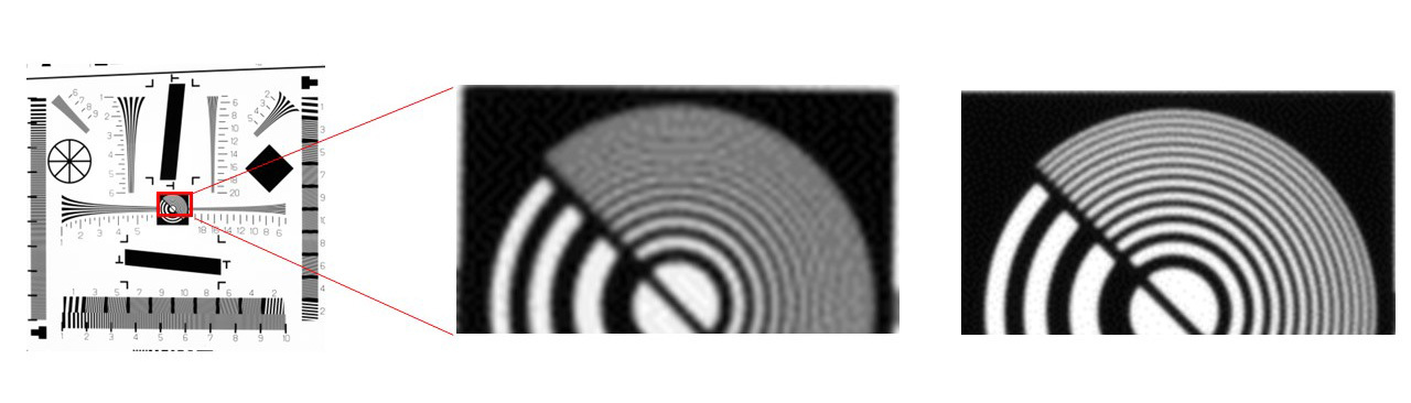
Comparison of SWIR images with different resolutions: Lighting wavelength 1550 nm (Left: Other SSS product, 1.34 effective megapixels; Right: IMX992)
■ Low-noise imaging even in dark locations possible by switching the shooting mode
Inclusion of new shooting modes enables low-noise imaging without being affected by environmental brightness. In dark environments with limited light, High Conversion Gain (HCG) mode directly amplifies the signal with minimal noise after being converted to an electrical signal from light, thereby relatively reducing the amount of noise downstream. Doing so minimizes the impact of noise in dark locations, leading to greater recognition precision. On the other hand, in bright environments with plenty of light, Low Conversion Gain (LCG) mode enables imaging prioritizing the dynamic range.
Furthermore, enabling Dual Read Rolling Shutter (DRRS) outputs images from the sensor in two distinct types. These images are then composited on the camera to acquire an image with significantly reduced noise.

Image quality and noise comparison in dark location: Lighting wavelength 1450 nm (Left: Other SSS product, 1.34 effective megapixels; Center: IMX992, HCG mode selected; Right: IMX992, HCG mode selected, DRRS enabled)
■ Optimized pixel structure for high-sensitivity imaging across a wide range
SSS’s SWIR image sensors employ a thinner indium-phosphorous (InP) layer on top, which would otherwise inevitably absorb visible light, thereby allowing visible light to reach the indium-gallium arsenide (InGaAs) layer underneath, delivering high quantum efficiency even in the visible wavelength. The new products deliver even higher quantum efficiency by optimizing the pixel structure, enabling more uniform sensitivity characteristics across a wide wavelength band from 0.4 to 1.7 μm. Minimizing the image quality differences between wavelengths makes it possible to use the image sensor in a variety of industrial applications and contributes to improved reliability in inspection, recognition, and measurement applications.
Related Links
Information on SenSWIR™, SSS’s short-wavelength infrared image sensor technology:
https://www.sony-semicon.com/en/technology/industry/senswir.html
IMX992 and IMX993 product website:
https://www.sony-semicon.com/en/products/is/industry/swir/imx992-993.html


