March 06, 2023
Atsugi, Japan — Sony Semiconductor Solutions Corporation (SSS) today announced the upcoming release of the IMX611, a direct time-of-flight (dToF) SPAD depth sensor for smartphones that delivers the industry’s highest photon detection efficiency.
The IMX611 has a photon detection efficiency of 28%, the highest in the industry, thanks to its proprietary single-photon avalanche diode (SPAD) pixel structure. This reduces the power consumption of the entire system while enabling high-accuracy measurement of the distance of an object.
This new sensor will generate opportunities to create new value in smartphones, including functions and applications that utilize distance information.
In general, SPAD pixels are used as a type of detector in a dToF sensor, which acquire distance information by detecting the time of flight of light emitted from a source until it returns to the sensor after being reflected off an object.
The IMX611 uses a proprietary SPAD pixel structure that gives the sensor the industry’s highest photon detection efficiency, at 28%, which makes it possible to detect even very weak photons that have been emitted from the light source and reflected off the object. This allows for highly accurate measurement of object distance. It also means the sensor can offer high distance-measurement performance even with lower light source laser output, thereby helping to reduce the power consumption of the whole smartphone system.
This sensor can accurately measure the distance to an object, making it possible to improve autofocus performance in low-light environments with poor visibility, to apply a bokeh effect to the subject’s background, and to seamlessly switch between wide-angle and telephoto cameras. All of these capabilities will improve the user experience of smartphone cameras. This sensor also enables 3D spatial recognition, AR occlusion, motion capture/gesture recognition, and other such functions. With the spread of the metaverse in the future, this sensor will contribute to the functional evolution of VR head mounted displays and AR glasses, which are expected to see increasing demand.
Main Features
■ Highly accurate distance measurement and low-power consumption made possible by the industry’s highest photon detection efficiency
The IMX611 employs a stacked configuration, where a Cu-Cu connection is used to achieve conduction for each pixel between the back-illuminated SPAD pixel chip (top) and the logic chip equipped with a distance measuring processing circuit (bottom). By arranging the circuit under the pixel chip, SSS has achieved a pixel size of 10 μm square, which is quite small for an SPAD, while still securing a high aperture ratio. SSS has also made the following improvements to the pixels:
・Use of a light incidence plane with irregularities on its surface to refract incident light, thereby enhancing the absorption rate
・Efficient multiplication via optimization of the design of the avalanche region in the pixel
These proprietary pixel structures combine to deliver the industry’s highest photon detection efficiency, at 28%, when using a wavelength of 940 nm, which is commonly used in laser light sources for smartphones. This enables highly accurate recognition and reduces the power consumption of the overall system.
■ Proprietary signal processing function simplifies overall system development
By incorporating a proprietary signal processing function into the logic chip inside the sensor, the RAW information acquired from the SPAD pixels is converted into distance information to output, and all this is done within the sensor. This approach makes it possible to reduce the load of post-processing, thereby simplifying overall system development.
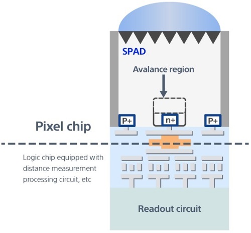
Structure of SPAD ToF depth sensor
More information about the applications utilizing ToF technology:
https://www.sony-semicon.com/en/application/mobile/sensing.html
More information on LYTIA mobile image sensors:
https://www.sony-semicon.com/en/products/is/mobile/index.html
Key Specifications
| Model name | IMX611 |
|---|---|
| Effective pixels | 140 x 170, 23,000 pixels |
| Image size | Diagonal 2.2 mm (1/8.1-type) |
| SPAD unit cell size | 10.08 x 10.08 µm |
| Recommended light source wavelength | 940 nm |
| Photon detection efficiency | 28% |
| Power consumption at 8m (long-distance mode) | 110mW (sensor) 160mW (system) |
| Distance precision | Less than 0.1% error |
| Distance signal processing | Included in the sensor’s logic chip |


