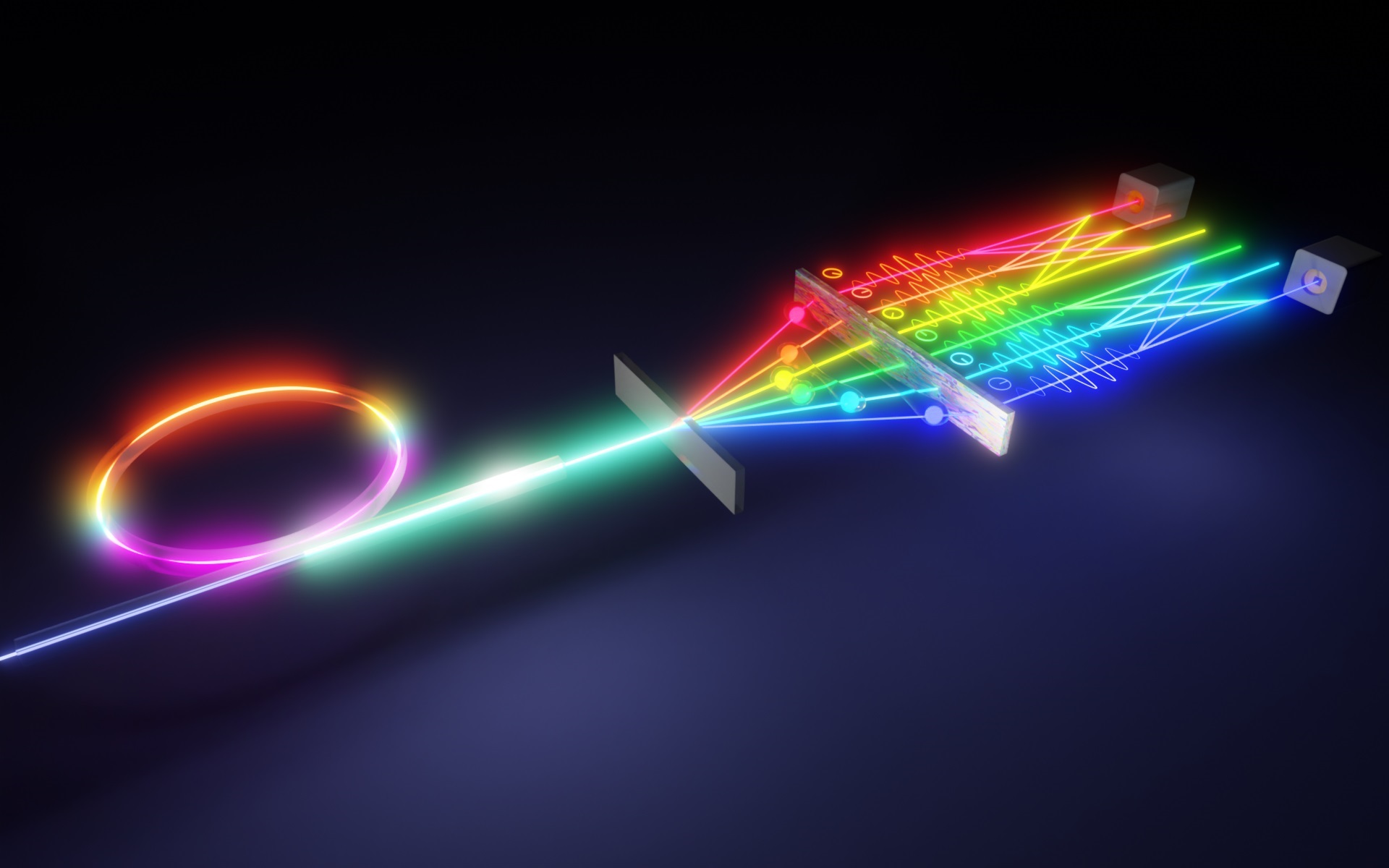
New York, N.Y. – September 21, 2016 – A recently issued U.S. Patent covers a revolutionary concept in a high- definition mega-pixel camera that can literally be flattened to about the thickness of a postage stamp. The “nanoCam” (as the inventor calls it) replaces the external lens to focus the image and collapses the entire apparatus into a sandwich including induction or battery-powered circuitry, printed pixel and lens array. Each tiny lens rests over a sensor layer of a number of pixels depending on the limit of the lens. Each of these nano-assemblies becomes a nano-sized camera receiving fuzzy or ‘noisy’ images. However the entire assembly of multiple mini cameras is sharpened through computerized interpolation transformation of each of the images to present the observer with a single high-resolution image. Since each element receives slightly different spatial information from the observed object, it also becomes possible to render 3D imaging and depth information.
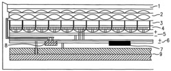
The nanoCam features a micro thin sandwich cross section, 360° fly’s eye, and scattered GPS-type invisible array.
Today’s digital cameras have been reduced to the smallest possible size they can by using current technology. Digital cameras require a conventional external lens to focus the image, light-harvesting elements to increase efficiency or perform “plenoptic” functions, and a light-sensitive CMOS/CCD layer that collects the image. The requirement of these critical elements severely limits how small a digital camera can be without significant loss of image quality. The nanoCam performs all of these functions in a totally flat package, enabling it to be just a fraction of the size of the smallest digital camera. The camera will accommodate various wide angle to telephoto focal lengths in sectors of the small chip.
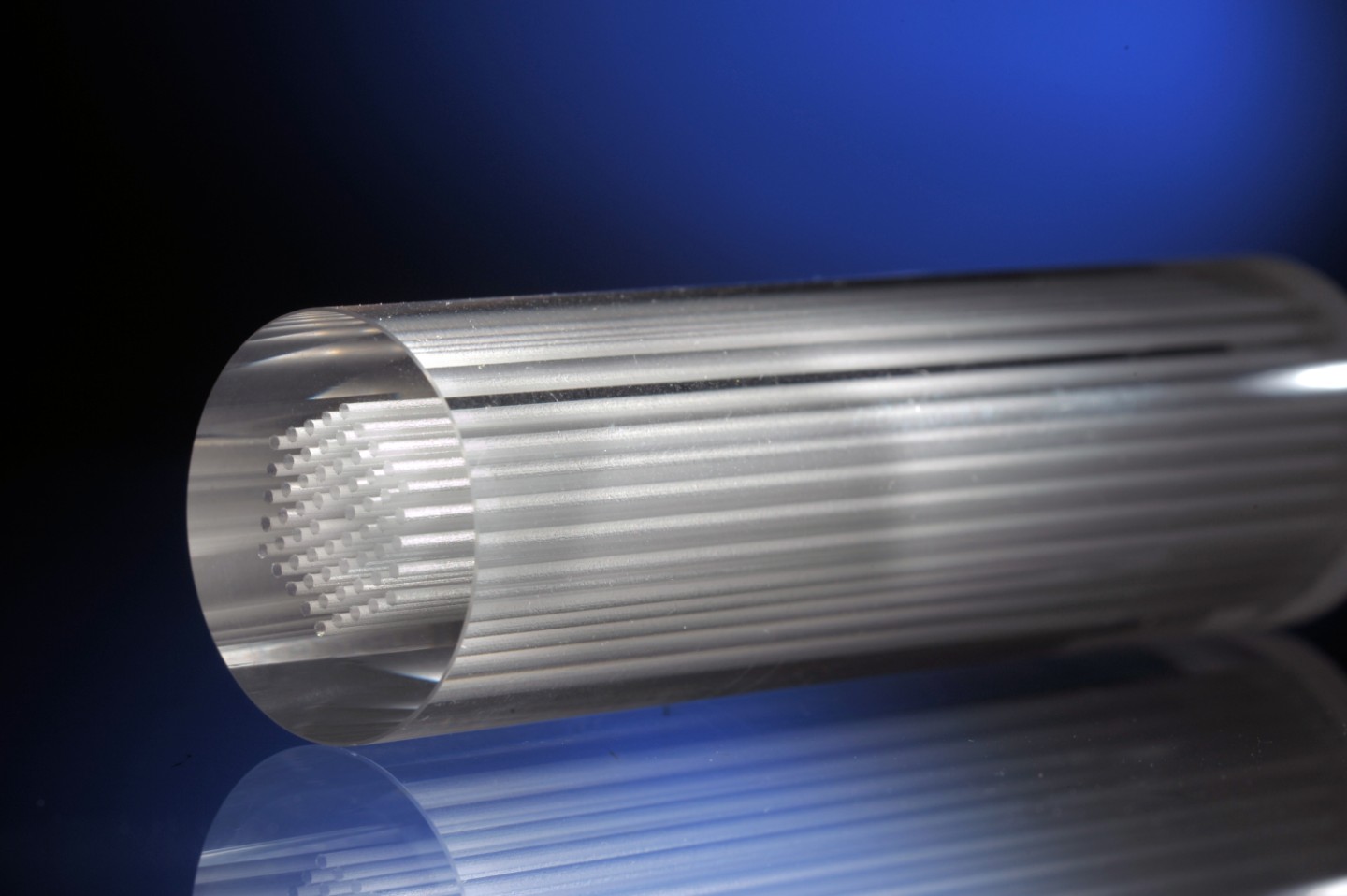
The technology behind the nanoCam is covered by U.S. Patent No. 8,077,245 for an “Apparatus for Imaging Using an Array of Lenses.” The patent covers an imaging system/camera consisting of multiple nano-sized optical elements arranged in an array format with more than one pixel per optical element, and will have a higher resolution than each element would be capable of individually, since each element, being at a different point, gathers slightly different overlapping information. Hence by processing such information one can obtain a clear image. Furthermore, multiple information from an array of sensors can be processed to obtain 3-D, stereotypic and panoramic imaging and may be connected to each other to enable seeing around obstacles as well as full three-dimensional tracking and/or metric determination of an unknown object.
Utilizing equally sized lenses and narrow bandwidth multi-wavelength sensing layers below the lenses can make color/spectroscopic images or by taking advantage of unique optical properties of micron 1000nm and smaller lenses accepting various wavelengths below their diffraction limits.
Applications for the nanoCam include consumer cameras on a contact lens, security and surveillance, medical electronics and diagnostics, endoscopy, cell and smart phones, and medical research to name just a few! “As this groundbreaking technology matures, it will undoubtedly lead to endless applications,” according to Dr. Thomas J. Adamo, lead inventor of the patent. Dr. Adamo has had a lifelong interest in physics, science fiction and was inspired by 3D printed nano machines. He was reading Arthur Clarke’s “Rendezvous with Rama” when a challenging thought experiment came to him: Just how small and invisible could a camera be? He recognized that unlike in the case of nano mechanics, the camera image would degrade to the point of uselessness as the size shrunk. The resulting thought experiment yielded that an integrated array of cameras was the answer. He consulted with a friend who was head of the Department of Nanophysics at a leading university to vet the idea and made him co-inventor.
The nanoCam intellectual property is currently assigned to nano-Light Technologies LLC. Inquiries regarding commercialization of the nano-Cam patent should be directed to Alec Schibanoff at alec@IPOfferings.com or 845-377-6911.