
19.08.2026
Photonic chips are undergoing continuous miniaturization. Today’s components are small enough to fit on a fingernail, yet capable of generating, manipulating and measuring light. To produce a specific optical effect, photonic chips typically rely on a single, specific material. Researchers at the Max Planck Institute for the Science of Light (MPL) have now used two different materials within the same component, thereby combining two nonlinear optical effects. The results, recently published in Advanced Photonics, demonstrate how materials with complementary properties can work together and expand the capabilities of integrated photonic circuits. This approach could inform future applications ranging from high-resolution spectroscopy and telecommunications to LiDAR and supercontinuum generation.
Photonic chips made of hybrid materials
Nonlinear optics describe how intense light changes the way a material responds to it. These interactions between light and material can generate new colors and frequencies of light and are of central importance for technologies such as optical frequency combs, spectroscopy and optical communication.
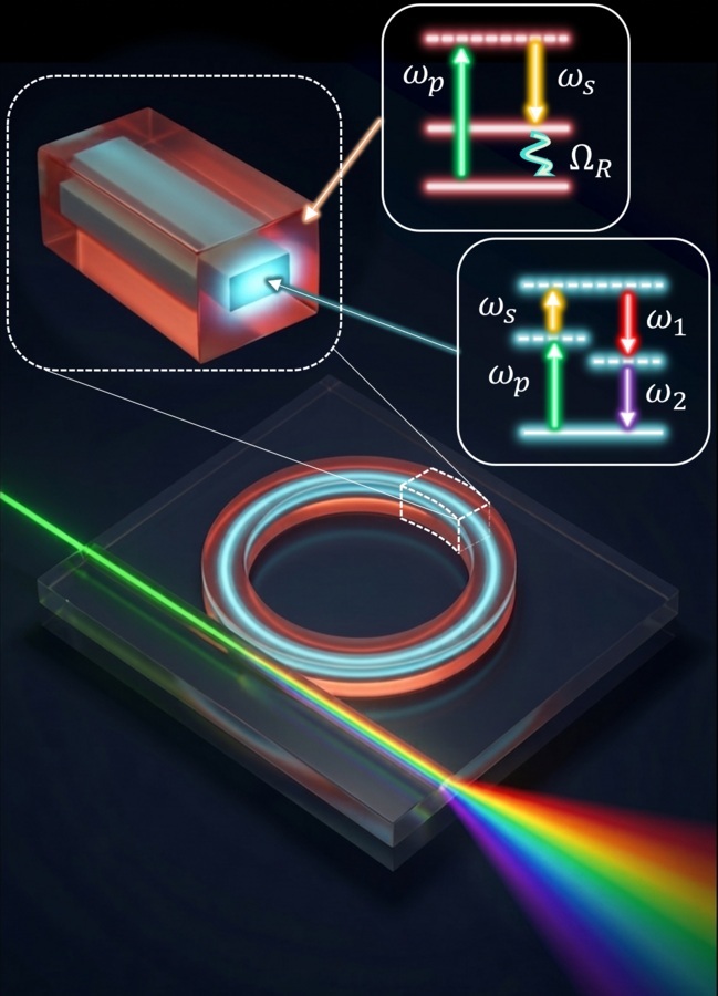
Most integrated photonic circuits guide light through a core material, while the cladding primarily serves to confine the light. Scientists from the “Microphotonics” research group, led by Dr. Pascal Del’Haye, have now designed a device in which light can interact with both the core and the cladding.
The device consists of a silicon nitride ring resonator surrounded by quartz (silicon dioxide). Ring resonators are capable of storing light for up to one million cycles. One-third of the circulating optical field extends into the quartz cladding. This overlap allows the different optical properties of the two materials to manifest simultaneously and complement or reinforce one another.
The quartz glass of the cladding provides Raman amplification, a process in which light interacts with molecular vibrations and emerges at a new frequency. In contrast, the silicon nitride in the core exhibits strong Kerr nonlinearity, which can generate optical frequency combs – precisely spaced sequences of light frequencies, also known as an “optical ruler.”
Silicon nitride is already widely used in integrated photonics due to its low optical losses and broad operating range. By allowing a portion of the light to interact with the surrounding silicon dioxide of the cladding, the scientists succeeded in introducing sufficient Raman gain into the silicon nitride platform to generate Raman laser emission.
From Raman Signals to Broad Frequency Combs
To test the concept, the researchers pumped the ring resonator with a laser and were able to measure a color shift in the laser caused by Raman scattering in quartz glass.
As the input power was further increased, the device exhibited another nonlinear process. Four-wave mixing in the silicon nitride core generated additional frequencies around both the original pump light and the light produced by Raman scattering.
Ultimately, these frequencies multiplied into broad optical frequency combs. By adjusting the dimensions of the silicon nitride waveguide, the researchers changed how different wavelengths travelled through the resonator and improved the interaction between the optical modes.
The optimized device generated frequency combs spanning more than 400 nanometers, with comb lines appearing not only around the pump wavelength but also at several Raman-shifted wavelengths.
The Cladding as Part of the Device
“The experiments show that a layer normally considered a support structure can become an active component of a photonic device. Instead of a single material having to provide all the desired optical properties, our approach allows different materials to contribute the functions they perform best,” says Arghadeep Pal, the paper’s lead author and a Ph.D. student in the Del’Haye Research Lab. “Just as people with different areas of expertise can achieve more through collaboration, materials with different strengths can work together to unlock new possibilities.”
The device achieved an energy conversion efficiency of over 32%. The researchers believe that further technical optimizations could improve coherence without compromising high efficiency.
“What surprised us was how strongly the cladding contributed to the device’s nonlinear behavior,” says Prof. Shuangyou Zhang, a co-author of the study who worked at MPL and is currently conducting research at the Technical University of Denmark.
The approach points to a more general design principle for integrated photonics: combining materials with different nonlinear properties could open new avenues for generating and controlling light on a chip. Similar hybrid systems could potentially enable broadband supercontinuum sources, self-referenced frequency combs, and other nonlinear photonic technologies.
“Hybrid integration gives us a powerful new degree of freedom in designing efficient and versatile nonlinear photonic circuits,” says Del’Haye.
By enabling the silicon nitride core and the silicon dioxide cladding to interact – rather than treating the cladding merely as a passive layer – the researchers have demonstrated a new way to expand the capabilities of integrated photonic circuits.
Original Publication in Advanced Photonics
Arghadeep Pal, Alekhya Ghosh, Shuangyou Zhang, et al. “Hybrid nonlinear effects in photonic integrated circuits,” Advanced Photonics 8(4), 046008 (23 Jun 2026).