28/07/2025
Metalenses, composed of subwavelength nanostructures that manipulate light, are celebrated for their potential to replace bulky optical components. Their unique functionalities—ranging from improved imaging resolution to advanced beam shaping—have spurred interest in applications from augmented reality to LiDAR systems. However, their fragility under mechanical stress and environmental exposure remains a barrier to commercialization. Traditional materials often fail to provide both optical performance and robustness, especially under visible light. Furthermore, the accumulation of dust and particles over time degrades metalens performance. Due to these challenges, there is a critical need to develop encapsulation strategies that offer mechanical protection and self-cleaning functionality without sacrificing optical efficiency.
A research team from Pohang University of Science and Technology has introduced a new encapsulation approach for metalenses, published (DOI: 10.1038/s41378-025-00925-3) on June 10, 2025, in Microsystems & Nanoengineering. The study details how they engineered spin-on-glass coated a-Si:H metalenses that are not only mechanically robust but also capable of passive self-cleaning. Through precise control of deposition parameters, the researchers optimized the refractive index of a-Si:H and successfully fabricated metalenses with conversion efficiencies up to 97.2%, while demonstrating strong resistance to physical damage and environmental contamination.
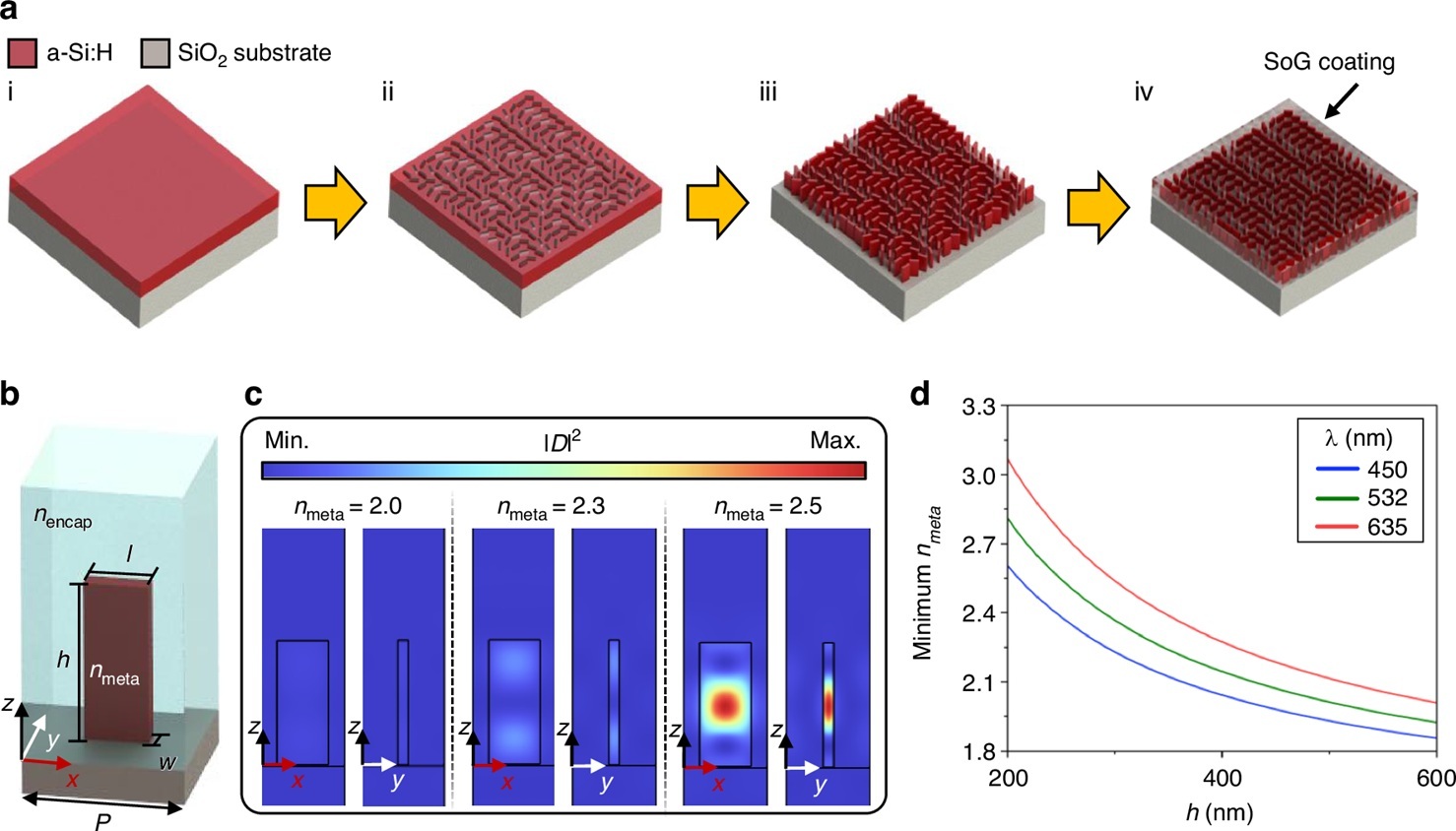
The team employed plasma-enhanced chemical vapor deposition (PECVD) to deposit a-Si:H films with tunable refractive indices, achieving a peak value of 3.23 at 635 nm by adjusting chamber pressure. These films were patterned into metalens structures via electron beam lithography and encapsulated using methyl silsesquioxane (MSQ), a spin-on-glass material that solidifies into a protective silica-like layer. Optical simulations and experimental results confirmed that high-index contrast between the meta-atoms and the SoG background enabled effective light manipulation. The encapsulated metalenses demonstrated remarkable durability: after 120 minutes of ultrasonic agitation with sand, they showed minimal damage and maintained over 56% conversion efficiency, while unencapsulated lenses suffered severe degradation. Furthermore, surface treatments enabled tunable wettability—from hydrophilic (7° contact angle) to superhydrophobic (116.2°)—allowing water droplets to roll off and remove contaminants, effectively enabling self-cleaning. These combined properties address the key limitations of current metasurface designs and mark a step forward in making metalenses viable for real-world use.
"Metalenses have always held tremendous promise, but fragility and cleanliness have been major hurdles," said Professor Junsuk Rho, corresponding author of the study. "Our encapsulation strategy not only preserves high optical performance but also adds durability and self-maintenance, bringing metalenses closer to integration in consumer electronics, imaging systems, and harsh environments. This work is a foundational leap toward making flat optics industrially practical."
These encapsulated metalenses offer an attractive solution for next-generation optical systems that demand compactness, efficiency, and resilience. Their self-cleaning ability is particularly relevant for applications in outdoor imaging, environmental sensors, and wearable optics, where exposure to dust and moisture is inevitable. Moreover, their mechanical robustness makes them suitable for integration into mobile devices, autonomous vehicles, and space equipment. With future developments in scalable manufacturing, such as nanoimprinting or UV lithography, these devices could be mass-produced cost-effectively, accelerating the commercialization of metasurface-based optics across a broad range of industries.
References
DOI
Original Source URL
https://doi.org/10.1038/s41378-025-00925-3
About Microsystems & Nanoengineering
Microsystems & Nanoengineering is an online-only, open access international journal devoted to publishing original research results and reviews on all aspects of Micro and Nano Electro Mechanical Systems from fundamental to applied research. The journal is published by Springer Nature in partnership with the Aerospace Information Research Institute, Chinese Academy of Sciences, supported by the State Key Laboratory of Transducer Technology.


