- Professor Jong Seok Lee's research team in the Department of Physics and Photon Science, in collaboration with the research team at the University of Minnesota, observed 'light-electron interaction anisotropy' in picosecond units in oxide thin films, and also succeeded in controlling the intensity of lightelectron interaction by adjusting the thickness of atomic layers
- Expected to be applied to next-generation large-area optoelectronic and spin devices...
Published in the international academic journal 《Science Advances》
The Gwangju Institute of Science and Technology (GIST, President Kichul Lim) announced that Professor Jong Seok Lee’s research team in the Department of Physics and Photon Science observed ultrafast ʻlightelectron interaction anisotropy*’ in picosecond (10-12 s) units in a ruthenium oxide (RuO2)* thin film for the first time in the world through joint research with the University of Minnesota, USA, and demonstrated that its intensity can be precisely controlled by adjusting the thickness of the atomic layer.
This study experimentally demonstrated for the first time that light-electron interaction anisotropy comparable to van der Waals materials can be implemented and controlled in metal oxides. It is evaluated that this has laid the foundation for the core technology required for the development of next-generation large-area optoelectronic devices.
Optoelectronic devices that utilize the interaction between light and electrons within solids are devices that create electrical signals with light or emit light with electricity, and are essential elements for various technologies in the field of electrical signal transmission, such as ultra-high-speed optical communications and optical imaging.
In particular, ʻoptical anisotropy’, which can control electronic signals depending on the polarization direction of light, is attracting attention as a key element of next-generation optical communications, imaging, and spintronics technologies.
To develop these devices, materials must be thin at the nanometer (10-9 m) level and capable of largearea production.
Until now, light-electron interaction anisotropy has been observed mainly in two-dimensional van der Waals materials, but industrial applications have been limited due to difficulties in large-area manufacturing and environmental instability.
On the other hand, metal oxides have the advantage of simultaneously achieving precise large-area growth at the atomic layer level and high environmental stability. If optical anisotropy is realized in these oxides, they have great potential as next-generation optoelectronic devices.
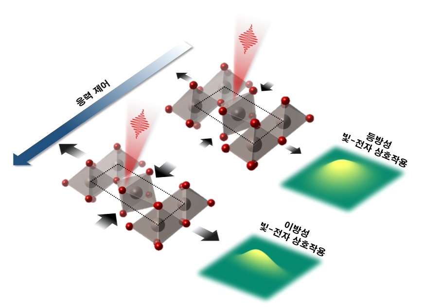
The research team confirmed the existence of light-electron interaction anisotropy at the level of van der Waals materials in ruthenium oxide thin films grown on titanium oxide (TiO2) substrates at atomic-levels using molecular beam epitaxy (MBE)* technology, through various optical measurements.
In addition to analyzing the static anisotropy of the material using X-ray absorption spectroscopy* and ellipsometry*, they observed that the behavior of photoexcited electrons significantly changed in picosecond (10-12 s) time units depending on the polarization direction using femtosecond laser-based pump-probe technology*. This is an important clue showing that ruthenium oxide thin films can be used for ultra-high-speed optoelectronic devices.
In addition, it was confirmed that by precisely controlling the thickness of the thin film at the atomic level and relieving the stress of the substrate, the strength of the light-electron interaction anisotropy can also be controlled. This is evaluated as an achievement that suggests a new direction for the design of oxide-based optoelectronic devices.
Professor Jong Seok Lee stated, “We have experimentally confirmed that the electronic structure can be controlled by utilizing stress in ruthenium oxide, which has recently attracted attention in the field of spintronics,” and added, “The results of this research will be an important starting point for the development of not only optoelectronic devices but also next-generation spin devices.”
This research was conducted as an international joint research between GIST and the University of Minnesota. At GIST, Professor Jong Seok Lee led the research, and Dr. In Hyeok Choi conducted an ultra high-speed optical experiment. At the University of Minnesota, Professor Bharat Jalan’s research team from the Department of Chemical Engineering and Materials Science was in charge of the growth of ruthenium oxide thin films, and Professor Tony Low’s research team from the Department of Electrical and Electronic Engineering was in charge of the electronic structure theory analysis.
The research results, which received support from the National Research Foundation of Korea's Limit Challenge R&D Project and the Mid-career Researcher Support Project, the U.S. Department of Energy (DOE) and the National Science Foundation (NSF), were published online in the international academic journal 《Science Advances》 on June 27, 2025.
* ruthenium dioxide (RuO2): A metallic oxide composed of ruthenium (Ru), a platinum group metal, and oxygen (O), it is a material with excellent electrical conductivity and chemical stability. Its crystal structure is mainly rutile, and since electrons and ions move easily, it is used in various fields such as electrode materials, catalysts, sensors, and transparent electrodes. In particular, RuO2 has excellent conductivity and controllable optical properties, so it has recently been attracting attention in research on optoelectronic devices and quantum materials.
* optical-electronic interaction anisotropy: Refers to the phenomenon in which the interaction between light (photons) and electrons varies depending on the direction within the material. This phenomenon occurs when the crystal structure or electronic band structure of the material is asymmetrical depending on the direction, and the dynamics of electrons vary depending on the direction in which light enters. It can generally be prominent in van der Waals materials or metallic oxides with strong interactions.
* molecular beam epitaxy (MBE): A thin film deposition technique that precisely grows a thin film in atomic layers by spraying gaseous atoms or molecules in the form of a 'beam' on a substrate in an ultra-high vacuum. This method has a very slow growth rate, but it allows for precise thickness control and impurity control at the atomic level, so it can produce thin films with high quality crystal structures. It is mainly used in the development of semiconductors, quantum materials, and precision optoelectronic devices.
* x-ray Absorption Spectroscopy (XAS): This is an analytical technique that measures how much a specific atom absorbs x-rays, and identifies the oxidation state, electronic structure, and bonding state with surrounding atoms. It is widely used in materials science and nanotechnology because it can obtain physical and chemical information at the atomic level by irradiating a sample with x-rays of various energies and analyzing the changes in the characteristic energy absorbed by the atom.
* spectroscopic ellipsometry: This technique shines linearly or circularly polarized light on a material and measures how the polarization state changes after the light is reflected. This allows for precise calculation of optical constants such as reflectivity, phase difference, thickness, refractive index, and absorption coefficient. In particular, it is used as a tool for precise non destructive analysis of the optical properties of thin films.
* pump-probe technique: This technique divides an ultrafast laser pulse into two, one (pump beam) stimulates the sample, and the other (probe beam) observes the sample's response at a specific time interval. By changing the time delay between the pump and probe and measuring it, the physical and optical change process in very short time units (femtoseconds, 10-15 seconds) can be tracked in a time-resolved manner. It is used to elucidate ultrafast dynamics, electron transport, and energy transfer processes.


