
03.07.2023
by Oliver Morsch
Researchers at ETH have created an antenna for light sources on a chip using an unusual placement of a semiconductor material. In the future, efficient nanoscale LEDs and lasers could be produced in this way.
In brief
- Modern data transmission is based, among other things, on the fact that information can be sent quickly through optical fibers in the form of light beams.
- The light sources are technologically challenging. Researchers at ETH Zurich, Empa and Barcelona have now laid the foundations for tiny, efficient light sources.
- For their mini light sources, the researchers use rules of quantum mechanics and a surprising new antenna solution.
The fast switching and modulation of light is at the heart, among other things, of modern data transfer, in which information is sent through fibre optic cables in the shape of modulated light beams. It has been possible for several years now to miniaturise light modulators and to integrate them into chips, but the light sources themselves – light emitting diodes (LEDs) or lasers – still pose problems to engineers. A team of researchers at ETH Zurich led by Prof. Lukas Novotny, together with colleagues at EMPA in Dübendorf and at ICFO in Barcelona, have now found a new mechanism by which tiny but efficient light sources could be produced in the future. The results of their research have recently been published in the scientific journal Nature Materials.
Trying the unexpected
“To achieve this, we first had to try the unexpected”, says Novotny. For several years he and his coworkers have been working on miniature light sources that are based on the tunnel effect. Between two electrodes (made of gold and graphene in this case) separated by an insulating material, electrons can tunnel according to the rules of quantum mechanics. Under particular circumstances – that is, if the tunnel process is inelastic, meaning that the energy of the electrons is not conserved – light can be created.
“Unfortunately, the yield of those light sources is rather poor because the radiative emission is very inefficient”, explains postdoc Sotirios Papadopoulos. This emission problem is well-known in other areas of technology. In mobile phones, for instance, the chips that create the microwaves needed for transmission are only a few millimetres in size. By contrast, the microwaves themselves have a wavelength of around 20 centimetres, which makes them a hundred times larger than the chip. To overcome this difference in size an antenna is needed (which, in modern phones, is actually no longer visible from the outside). Likewise, in the experiments of the Zurich researchers the wavelength of the light is much larger than the light source.
Semiconductor outside the tunnel junction
“One might think, then, that we were consciously looking for an antenna solution – but in reality we weren’t”, says Papadopoulos. Like other groups before them, the researchers were investigating layers of semiconductor materials such as tungsten disulfide with a thickness of a single atom sandwiched between the electrodes of the tunnel junction in order to create light in this way. In principle one would assume that the optimal position should be somewhere between the two electrodes, maybe a little closer to one than to the other. Instead, the researchers tried something completely different by putting the semiconductor on top of the graphene electrode – completely outside the tunnel junction.
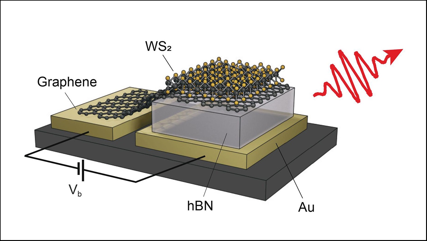
The semiconductor material (tungsten disulfide, WS2) placed outside the tunnel junction (right) acts as an antenna and makes it possible to enhance the energy created in the tunnel junction. (Illustration: Sotirios Papadopoulos / ETH Zurich)
Surprising antenna action
Surprisingly, this apparently illogical position worked very well. The researchers found out the reason for this by varying the voltage applied to the tunnel junction and measuring the current flowing through it. This measurement showed a clear resonance, which matched a so-called exciton resonance of the semiconductor material. Excitons are made of a positively charged hole, which corresponds to a missing electron, and an electron bound by the hole. They can be excited, for instance, by light irradiation. The exciton resonance was a clear sign that the semiconductor was not excited directly by charge carriers – after all, there were no electrons flowing through it – but rather that it absorbed the energy created in the tunnel junction and subsequently re-emitted it. In other words, it acted very much like an antenna.
Applications in nanoscale light sources
“For now, this antenna is not very good because inside the semiconductor so-called dark excitons are created, which means that not much light is emitted”, Novotny concedes: “Improving this will be our homework for the near future”. If the researchers are successful in making the light emission by the semiconductor more efficient, it should be possible to create light sources that measure only a few nanometres and are, thus, a thousand times smaller than the wavelength of the light they produce. As there are no electrons flowing through the semiconductor antenna, there are also none of the unwanted effects that typically occur at boundaries and that can reduce the efficiency. “In any case, we have opened a door to new applications”, says Novotny. Trying the unexpected has evidently paid off.
Reference
Wang, L, Papadopoulos, S, Iyikanat, F, Zhang, J, Huang, J, Taniguchi, T, Watanabe, K, Calame, M, Perrin, ML, García de Abajo, FJ, Novotny, L. Exciton-assisted electron tunnelling in van der Waals heterostructures. Nat. Mater. (2023). https://doi.org/10.1038/s41563-023-01556-7


