Oct. 26, 2021
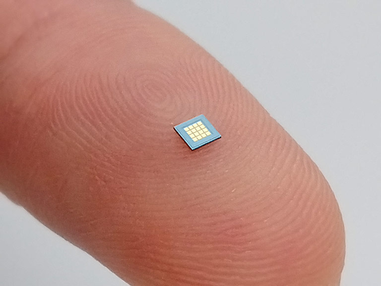
Hamamatsu Photonics has established high-density integration technology for iPMSELTM (integrable Phase Modulating Surface Emitting Laser) elements. These are the world’s smallest class semiconductor lasers capable of emitting light beams in 2D patterns. By leveraging this technology, we succeeded in developing an iPMSEL array consisting of 16 elements formed in 4 rows and 4 columns on a tiny chip only 2 millimeters square. Each iPMSEL element on the chip can be independently switched to emit light beams in various patterns making the iPMSEL array an ideal light source for industrial 3D shape measurement systems requiring very high accuracy. The iPMSEL array is also ideal for boosting motion capture and facial recognition accuracy. Moreover, their tiny size and light weight will also make them indispensable for compact handheld fiberscopes in medical and industrial fields.
A portion of this research and development work was supported by Japan Science and Technology Agency (JST) Center of Innovation (COI) Grant Number JPMJCE1311.
Product Overview
The iPMSEL array Hamamatsu Photonics has currently developed is capable of emitting light beams in various patterns that can form over 10,000 dots, fringes or stripes, grids, characters, CG and images, etc.
Hamamatsu Photonics has already developed iPMSEL elements based on a technology of the photonic crystal surface-emitting laser (*1) along with their unique hologram design and microfabrication technologies. So far, they have downsized the iPMSEL elements to a square shape of approximately 100 μm or micrometers (a micrometer is one-millionth of a meter), which is the world’s smallest class of semiconductor lasers capable of emitting light beams in 2D patterns. Taking advantage of their ultra-tiny size they mounted multiple elements at high density on a tiny substrate and demonstrated that these elements can emit light, while switching their beam patterns by electrically controlling individual elements.
Now, by applying iPMSEL element process technology, they have created a way to simultaneously form multiple iPMSEL 200 μm square elements at high density and with high accuracy onto a tiny chip. More specifically, they succeeded in fabricating a small iPMSEL array consisting of 16 elements arrayed in 4 rows and 4 columns at 300 μm spacing, on a chip only 2 millimeters square. This means they have formed more than 10 times the number of iPMSEL elements at high density in the same area as before, and also improved the position accuracy of each element to emit light beams while switching their patterns at high accuracy.
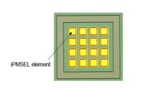
Enlarged view of iPMSEL array
The iPMSEL array consists of 16 iPMSEL elements, each a square of approximately 200 μm and formed at high density on a tiny 2 mm square chip. The iPMSEL array emits light beams while switching their beam patterns by electrical control of each individual element.
The iPMSEL array we have currently developed performs high precision measurements such as a phase-shifting method (*2), making it promising as a light source for industrial 3D shape measurement systems that require very high accuracy. The iPMSEL array can also be applied to motion capture and facial recognition to enhance their accuracy. Additionally, the tiny size and light weight achieved by high density integration technology will prove ideal for creating a vast product range including small, compact industrial fiberscopes and endoscopes for the medical field.
Hamamatsu Photonics will continue to improve its output efficiency to successfully commercialize these iPMSEL arrays and also strive to open up new application fields for iPMSEL elements.
Development Background
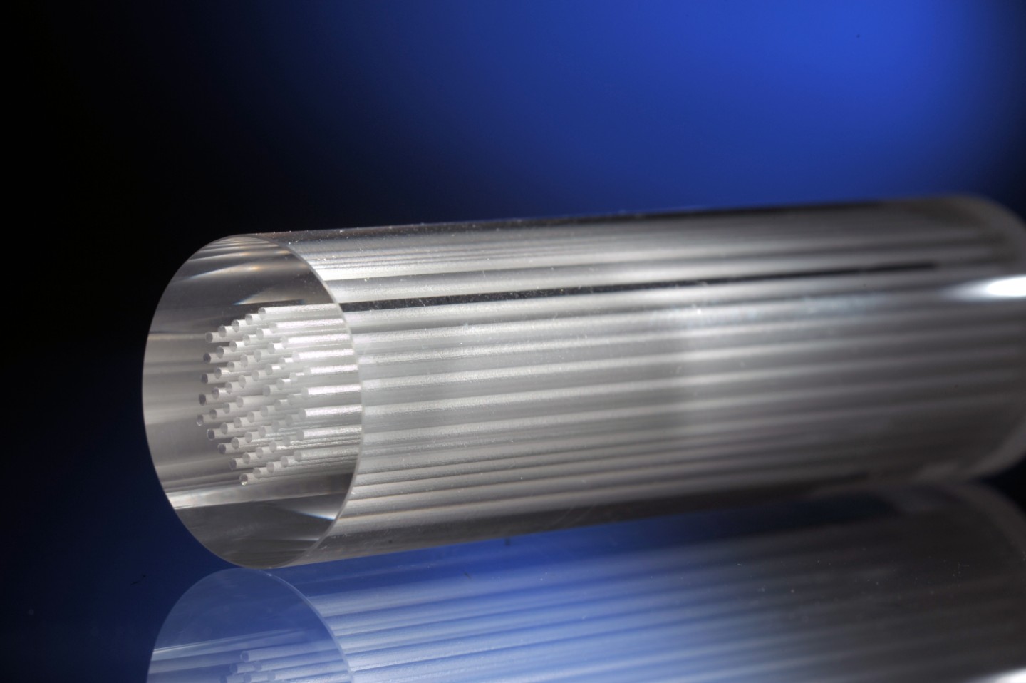
The 3D surface shape of an object can be measured by irradiating beam patterns onto the target object and capturing distortions in the beam patterns with a camera. This type of 3D shape measurement mainly utilizes a 2D beam pattern light source consisting of a vertical cavity surface emitting laser (VCSEL) and a diffractive optical element (DOE) that reshapes light from the VCSEL. To improve this approach we have been working to create high-density integration technology for small iPMSEL elements that are only about 1/10th the size of beam pattern light sources using VCSEL and DOE elements. This will help us create a chip-scale array of iPMSEL elements to serve as a light source ideal for highprecision 3D shape measurement.
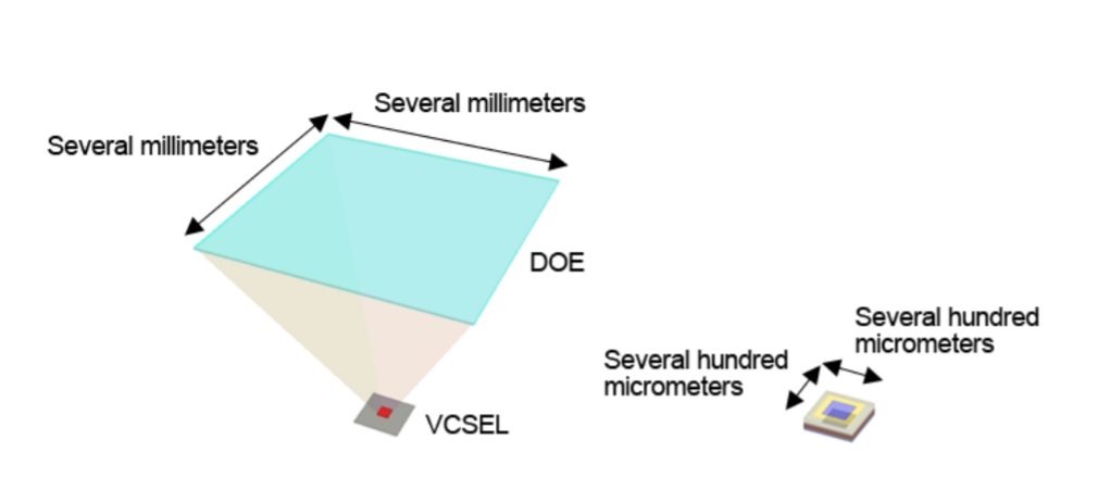
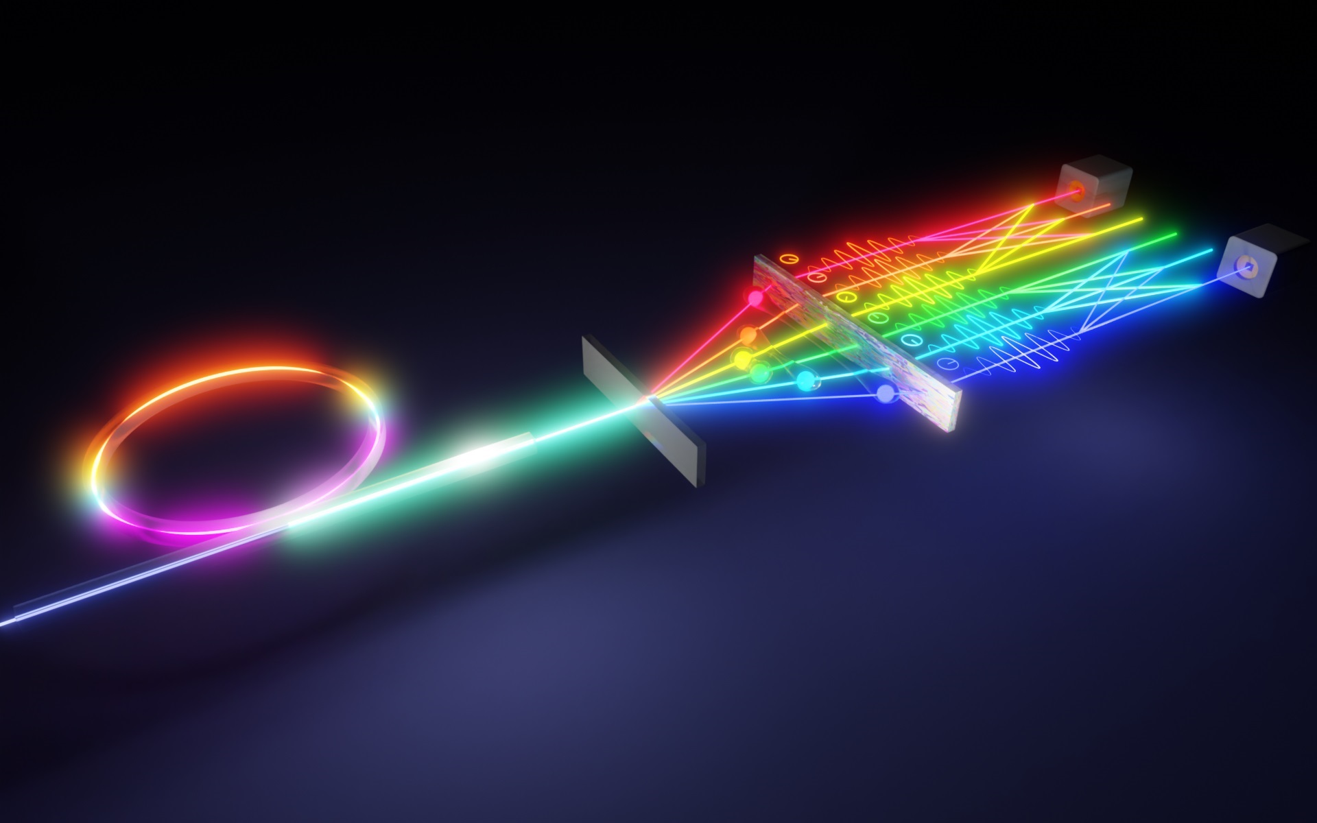
Concept image of a beam pattern light source (left) consisting of VCSEL, DOE and iPMSEL element (right)
*1 Photonic crystal surface-emitting laser: A surface-emitting laser which utilize the 2D photonic crystal (structure where microstructures are aligned in space equivalent to a wavelength of light) as a resonator which is developed by Prof. Noda’s group in Kyoto university.
*2 Phase-shifting method: This is a technique for measuring the 3D surface shape of an object with high accuracy, by irradiating periodic 2D beam patterns onto the object and analyzing distortions in the beam patterns that occur depending on the shape of the object.