June 13, 2019
Stanford, CA – Led by Jonathan Fan, an assistant professor in the department of Electrical Engineering, the team has designed and demonstrated ultrathin lenses, termed metalenses, with focusing efficiencies greater than 90%. This type of device is a promising technology for constructing lightweight and compact optics.
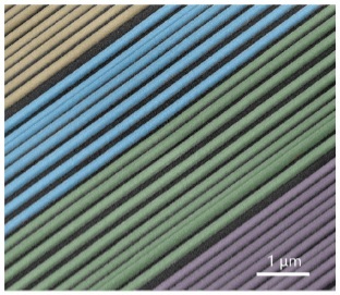
Whereas typical lenses are bulky, curved pieces of glass, these novel devices are made of carefully engineered nanostructures. Up to now, however, the efficiencies of metalenses have been too low for them to be useful in practical applications. Fan’s group has been able to circumvent these limitations by developing a new approach to the design problem, based on optimization, which is scalable and high performing. “Metamaterials are traditionally designed using intuition and heuristics,” said Fan. “While these methods are relatively easy to implement, they don’t provide the performance required of today’s demanding optical systems.”
While numerical optimization has been a known route to improving the performance of optical devices such as metamaterials, it requires extensive computational resources and cannot practically scale to large area devices. To tackle this problem, Fan’s team developed a divide-and-conquer approach. Rather than attempting to optimize the entire metalens at once, they first subdivided the device into many small sections. Each section, which behaves as a directional scatterer, is then designed for a particular optical response. Finally, all of the sections are recombined to produce the large area device.
“It turns out that optimizing many small, wavelength-scale structures is far faster than optimizing one big structure,” said Thaibao Phan, the lead author on the study. “The time to design a millimeter-scale device can be reduced over 100 fold with our approach. By leveraging the power of distributed computing, our optimization methods can be even further accelerated. These advances allow the practical development of high performance, large area metalenses.”
This optimization technique is general and can apply to other classes of diffractive optical devices beyond lenses, as well as other metamaterials. It paves the way to implementing nanoscale optical technologies operating at their design limits.
This work is supported by the Air Force Office of Scientific Research and the Office of Naval Research.
The full paper can be found here.