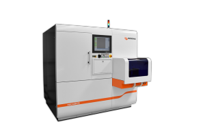
CHEMNITZ, Germany, July 6, 2016 – 3D-Micromac AG, a leading supplier of laser micromachining and roll-to-roll laser systems for the photovoltaic, medical device and electronics markets, today announced that its microDICE™ laser micromachining system has been adopted by a major industrial manufacturer for volume production of high-power diodes.
Leveraging 3D-Micromac’s proprietary TLS-Dicing™ technology, the microDICE system provides fast, clean and cost-effective dicing of wafers used for advanced semiconductors and power device applications. Its unique approach uses thermally induced mechanical stress to separate brittle semiconductor materials such as silicon, silicon carbide (SiC), germanium (Ge) and gallium arsenide (GaAs).
TLS-Dicing is a contact- and residue-free process that provides significantly higher throughput, higher yields and greater functionality compared to traditional die-separation technologies. For example, throughput is up to 30X greater compared to saw dicing. The technology also provides lower cost of ownership than other approaches. A forceless and contactless machining process, TLS-Dicing eliminates tool wear and requires no expensive consumables for surface cleaning—resulting in cost savings of up to an order of magnitude or more.
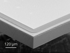
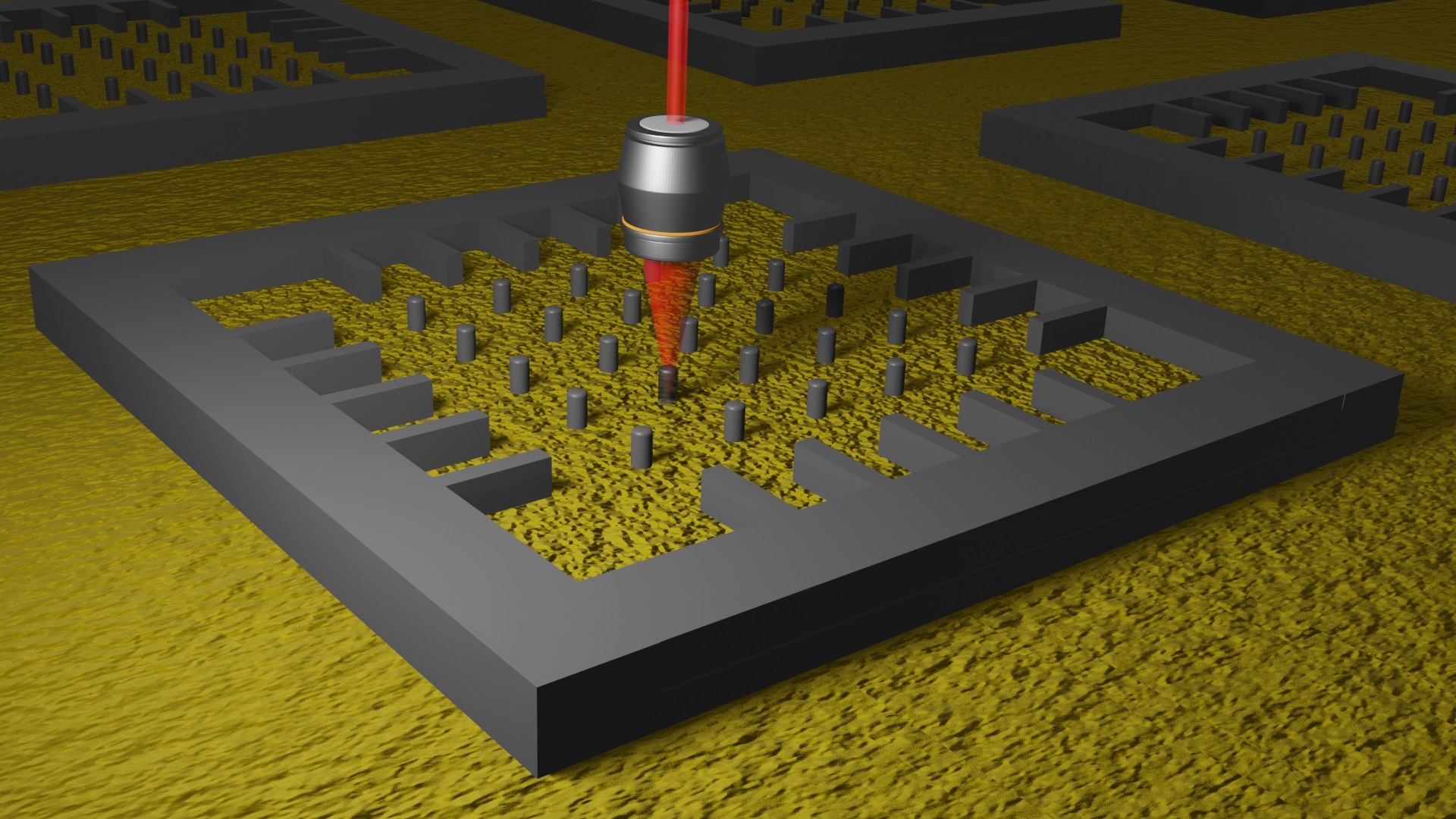
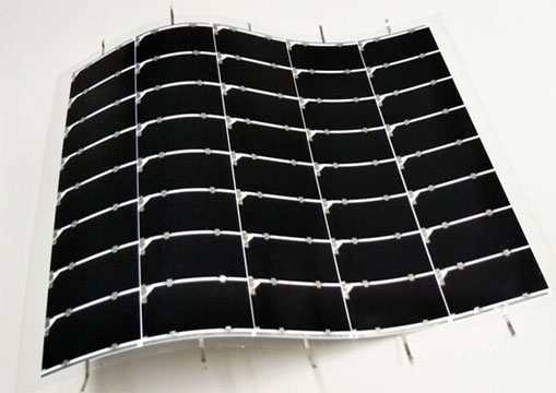
3D-Micromac’s proprietary TLS-Dicing™ technology on a Silicon Carbide (SiC) wafer provides die separation free of chipping, as well as enables back-side metal separation.
“While significant time and resources are invested in the front-end of semiconductor manufacturing to produce a completed product wafer, back-end wafer processing has historically been viewed as a necessary evil,” stated Tino Petsch, CEO of 3D-Micromac. “That’s all changed with the adoption of new types of wafer substrates, thinner wafers and scaling to smaller dimensions, larger-size substrates, and new packaging technologies like 3D-stacking. Back-end process steps such as wafer dicing are evolving as critical value-add process steps that not only ensure, but also further enhance, device yields. Using our TLS-Dicing technology, the microDICE system provides superior wafer dicing performance over other approaches while considerably reducing the dicing cost per wafer. Our technology has been proven in the photovoltaic and other industrial markets, and we are pleased to bring the benefits of it to the semiconductor and power device manufacturing industry.”
3D-Micromac also announced today that it is expanding its global infrastructure with the opening of its new 3D-Micromac America headquarters in the heart of Silicon Valley, in San Jose, Calif. Serving as both an applications lab and sales and support facility, the office marks the company’s first major presence in North America and will enable 3D-Micromac to better meet rising customer demand for its laser micromachining products across all of its served markets, including solar, semiconductor, MEMS, display and smart glass.
According to Daniel Weber, sales and business development manager for 3D-Micromac America, “With our new regional headquarters and applications lab, 3D-Micromac can offer our North American-based customers a first-class network of sales and support services for our laser micromachining systems. Providing customer evaluations, applications development, and small-scale contract manufacturing is a unique offering among wafer dicing technology suppliers. We look forward to delivering all of these capabilities to our existing, new and potential customers.”
3D-Micromac America, LLC is located at 2151 O’Toole Ave, #40, San Jose, CA 95131, Tel. +1-408-850-7252.
Other key advantages of 3D-Micromac’s microDICE system with TLS-Dicing versus traditional separation technologies include:
- No chipping or micro cracks – excellent cleaving results with no defects
- Particle-free – no debris discharge since the substrate is only heated and not vaporized
- Minimal heat-affected zones – other laser dicing approaches can generate unwanted heat that causes damage to the area around the site of the laser
- Increased yields – results in zero kerf (width of cut made by saw dicing), which leads to narrower scribe lines and frees up more real estate on the wafer for making product. It also has no negative impact on the electrical performance of the device, and in some applications it can improve performance, such as reducing leakage current on power diodes
- Fewer process steps – eliminates need for protective coating and adjacent cleaning process
- Excellent back-side metal separation – no peeling or delamination
- Processes up to 300-mm wafer substrates
Media, analysts and potential customers interested in learning more about 3D-Micromac’s laser micromachining solutions, including microDICE, are invited to visit the company’s booth #6452 in the North Hall of the Moscone Convention Center in San Francisco, Calif., at the SEMICON West show on July 12-14.
More information on the microDICE system can be downloaded at: http://3d-micromac.com/int/products/microdice/.
About 3D-Micromac AG
Founded in 2002, 3D-Micromac AG is the industry leader in laser micromachining, delivering powerful, user-friendly and leading edge processes with superior production efficiency. We develop processes, machines and turnkey solutions at the highest technical and technological level. 3D-Micromac systems and services have been successfully implemented in various high-tech industries worldwide including photovoltaic, semiconductor, glass and display industries, micro diagnostics, and medical technology. For more information, visit the company’s website at http://www.3d-micromac.com/