May 12, 2020
Contributing to the Development of Diverse Industrial Equipment by Delivering Compactness and Imaging over a Broad Range of Wavelengths
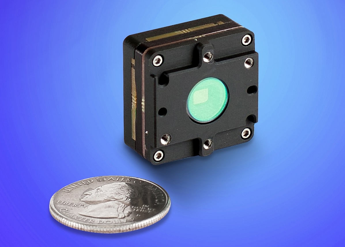
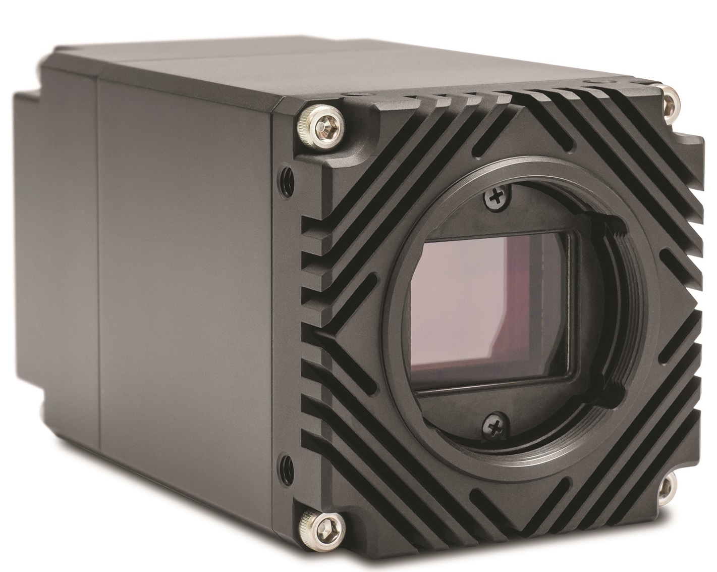
Tokyo, Japan — Sony Corporation today announced the upcoming release of two new models of short-wavelength infrared (SWIR) image sensors for industrial equipment. The new sensors are capable of capturing images in the visible and invisible light spectrum in the short-wavelength infrared range and boast a compact size made possible by the industry's smallest*1 5μm pixel size.
The new products employ Sony's original SenSWIR*2 technology, in which photodiodes are formed on an indium gallium arsenide (InGaAs) compound semiconductor layer and are connected via Cu-Cu connection*3 with the silicon (Si) layer which forms the readout circuit — a design which enables high-sensitivity over a broad range of wavelengths. This breakthrough yields a SWIR image sensor that is compact yet capable of delivering seamless image capture over a broad range of wavelengths covering from the visible to invisible light spectrum in the short-wavelength infrared range (wavelength: 0.4μm to 1.7μm).
Employing these products enables sensing even in wavelengths not visible to the human eye, making possible the development of cameras and testing equipment for various applications and contributing to the development of diversifying industrial equipment.
The recent demand to reduce manpower and ensure standardization in the industrial equipment field is driving a growing need for image sensors capable of capturing images in the invisible light spectrum of the short-wavelength infrared range. However, traditional SWIR image sensors face manufacturing challenges in miniaturizing pixels and increasing pixel count, as well as various other issues including low sensitivity in the visible light spectrum and analog output that makes multifunctionality difficult. These factors have inhibited the penetration and increased applications of industrial cameras using conventional technology.
Sony's new sensors employ the stacking technology using Cu-Cu connection that Sony has developed for years along with Sony's original SWIR image sensor technology, delivering high image quality and a more compact sensor size thanks to miniaturization, as well as high sensitivity imaging in a broad range of wavelengths covering both the visible and invisible spectrum. The new products also support digital output, matching the performance of current CMOS image sensors for industrial equipment.
Going forward, Sony will propose these products for use in a wide range of industrial applications such as material selection, contaminant inspection, and semiconductor inspection, aiming to contribute to improved productivity.
Main Features
Compact, multi-pixel design made possible by the industry's smallest 5μm pixels
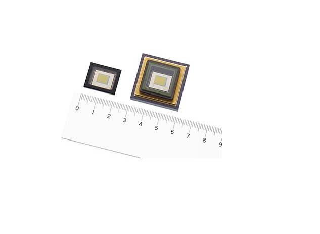
When bonding the InGaAs layer, which forms the light receiving photodiodes, and the Si layer, which forms the readout circuit, using conventional bump connections, it is necessary to secure a certain bump pitch, which makes it difficult to achieve a smaller pixel size compared to current industrial CMOS sensors. This had made miniaturization a serious challenge. The Sony's new products, however, feature a smaller pixel pitch made possible by the Cu-Cu connection, resulting in the industry's smallest 5μm pixel size. This, in turn, makes it possible to reduce camera size while maintaining SXGA (IMX990)/VGA (IMX991) resolution, contributing to improved testing precision.
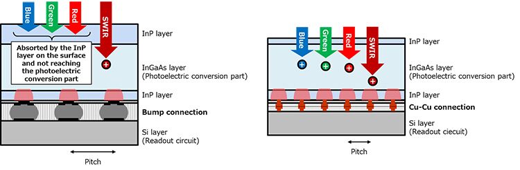
Left: Bump connection; Right: Cu-Cu connection
Imaging over a broad range of wavelengths covering both the visible and invisible light spectrums
Sony's original SWIR image sensor technology is used to make the top InP layer,*4 which absorbs visible light, thinner, making it possible to transmit light to the InGaAs layer underneath, delivering high quantum efficiency even in the visible range. This design enables imaging in a broad range of wavelengths from 0.4μm to 1.7μm, enabling the use of a single camera instead of the conventional multiple that were required to capture visible light and SWIR. This results in lower system costs and faster speeds thanks to the reduced image processing load, allowing for a dramatic expansion in testing range.
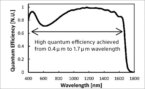
Wavelength (horizontal axis) and quantum efficiency (vertical axis) of the products
Imaging sample 1
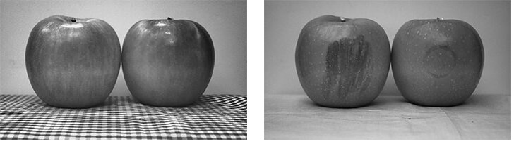
Switching light sources makes it possible to obtain the surface information and subsurface information of the apples simultaneously (left: visible light; right: short-wavelength infrared)
Imaging sample 2
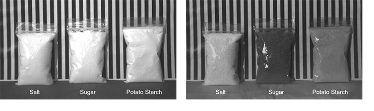
Material sorting utilizing differences in short-wavelength infrared light absorption rates (left: visible light; right: short-wavelength infrared)
Enhanced capabilities via digital output
Although conventional SWIR image sensors generally have an analog output, the new products support digital output to deliver the same performance as current industrial CMOS image sensors. Although analog output sensors require a digital conversion circuit or other functionality for industrial equipment on the camera, these products already include this functionality, reducing the number of steps in camera development and making multifunction camera development easier.
*1: Among SWIR image sensors using InGaAs. According to Sony research (as of announcement on May 12, 2020).
*2: The InGaAs layer, which forms the light-receiving photodiodes, and the Si layer, which forms the readout circuit, are connected via Cu-Cu connection. This allows the indium phosphide (InP) layer to be thinner, thereby permitting the penetration of visible light.
*3: Technology that provides electrical continuity via connected Cu (copper) pads when stacking the back-illuminated CMOS image sensor section (top chip) and logic circuits (bottom chip). Compared with through-silicon via (TSV) wiring, where the connection is achieved by penetrating electrodes around the circumference of the pixel area, this method gives more freedom in design, improves productivity, allows for a more compact size, and increases performance.
*4: Substrate that serves as a base for the InGaAs layer.