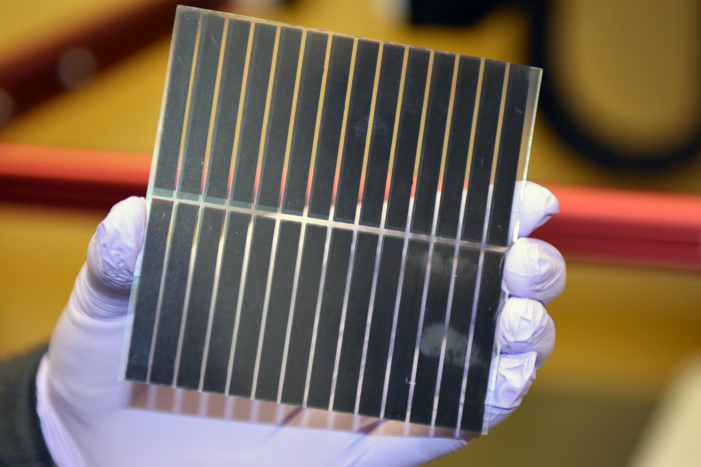
HOUSTON – (June 19, 2014) – Rice University scientists have created a one-step process for producing highly efficient materials that let the maximum amount of sunlight reach a solar cell.
The Rice lab of chemist Andrew Barron found a simple way to etch nanoscale spikes into silicon that allows more than 99 percent of sunlight to reach the cells’ active elements, where it can be turned into electricity.
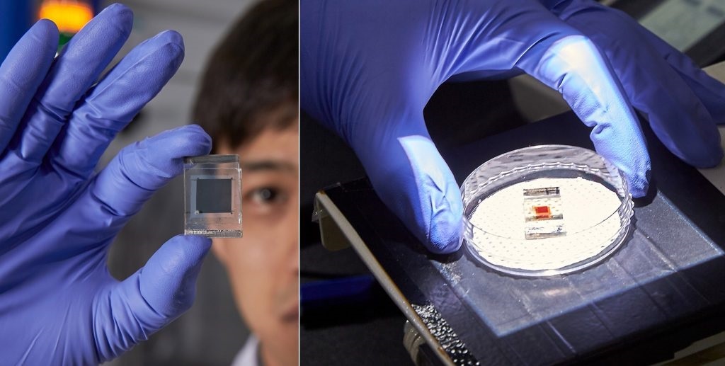
The research by Barron and Rice graduate student and lead author Yen-Tien Lu appears in the Royal Society of Chemistry’s Journal of Materials Chemistry A.
The more light absorbed by a solar panel’s active elements, the more power it will produce. But the light has to get there. Coatings in current use that protect the active elements let most light pass but reflect some as well. Various strategies have cut reflectance down to about 6 percent, Barron said, but the anti-reflection is limited to a specific range of light, incident angle and wavelength.
Enter black silicon, so named because it reflects almost no light. Black silicon is simply silicon with a highly textured surface of nanoscale spikes or pores that are smaller than the wavelength of light. The texture allows the efficient collection of light from any angle — from sunrise to sunset.
Barron and Lu have replaced a two-step process that involved metal deposition and electroless chemical etching with a single step that works at room temperature.
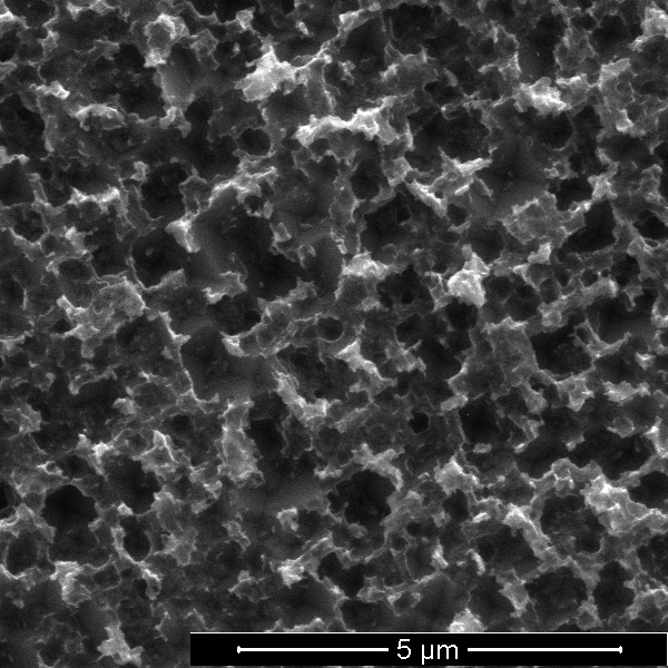
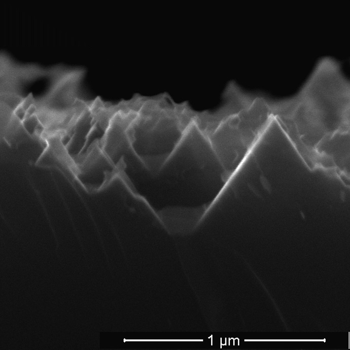
Rice University scientists have reduced to one step the process to turn silicon wafers into the black silicon used in solar cells. The advance could cut costs associated with the production of solar cells. Here, a top-down view shows pyramid-shaped pores etched into silicon over eight hours. (Credit: Barron Group/Rice University)
The chemical stew that makes it possible is a mix of copper nitrate, phosphorous acid, hydrogen fluoride and water. When applied to a silicon wafer, the phosphorous acid reduces the copper ions to copper nanoparticles. The nanoparticles attract electrons from the silicon wafer’s surface, oxidizing it and allowing hydrogen fluoride to burn inverted pyramid-shaped nanopores into the silicon.
Fine-tuning the process resulted in a black silicon layer with pores as small as 590 nanometers (billionths of a meter) that let through more than 99 percent of light. (By comparison, a clean, un-etched silicon wafer reflects nearly 100 percent of light.)
Barron said the spikes would still require a coating to protect them from the elements, and his lab is working on ways to shorten the eight-hour process needed to perform the etching in the lab. But the ease of creating black silicon in one step makes it far more practical than previous methods, he said.
Barron is Rice’s Charles W. Duncan Jr.–Welch Professor of Chemistry and a professor of materials science and nanoengineering.
Natcore Technology Inc., the Robert A. Welch Foundation and the Welsh Government Sêr Cymru Program supported the research.
Read the abstract at http://pubs.rsc.org/en/content/articlelanding/2014/ta/c4ta02006e#!divAbstract