HOUSTON – (Dec. 19, 2014) – An atomically thin material developed at Rice University may lead to the thinnest-ever imaging platform.
Synthetic two-dimensional materials based on metal chalcogenide compounds could be the basis for superthin devices, according to Rice researchers. One such material, molybdenum disulfide, is being widely studied for its light-detecting properties, but copper indium selenide (CIS) also shows extraordinary promise.
Sidong Lei, a graduate student in the Rice lab of materials scientist Pulickel Ajayan, synthesized CIS, a single-layer matrix of copper, indium and selenium atoms. Lei also built a prototype — a three-pixel, charge-coupled device (CCD) — to prove the material’s ability to capture an image.
The details appear this month in the American Chemical Society journal Nano Letters.
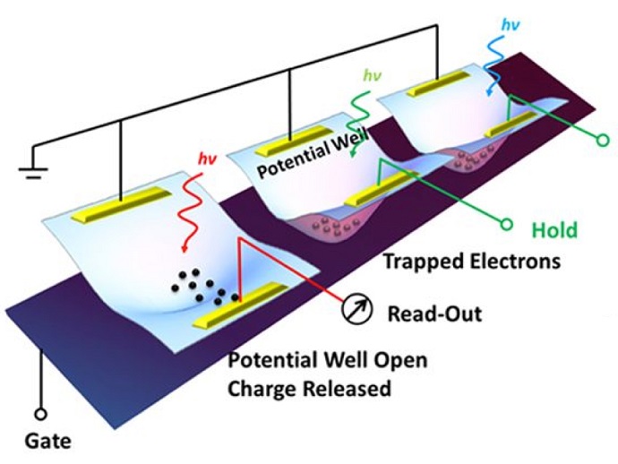
A schematic shows the design of an optoelectronic memory device based on CIS, a two-dimensional material developed at Rice University. The device traps electrons formed when light hits the material and holds them until released for storage; it could form the basis of future flat imaging devices. (Credit: Ajayan Group/Rice University)
Lei said the optoelectronic memory material could be an important component in two-dimensional electronics that capture images. “Traditional CCDs are thick and rigid, and it would not make sense to combine them with 2-D elements,” he said. “CIS-based CCDs would be ultrathin, transparent and flexible, and are the missing piece for things like 2-D imaging devices.”
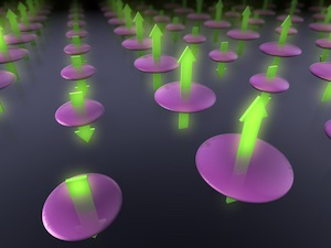
The device traps electrons formed when light hits the material and holds them until released for storage, Lei said.
CIS pixels are highly sensitive to light because the trapped electrons dissipate so slowly, said Robert Vajtai, a senior faculty fellow in Rice’s Department of Materials Science and NanoEngineering. “There are many two-dimensional materials that can sense light, but none are as efficient as this material,” he said. “This material is 10 times more efficient than the best we’ve seen before.”
Because the material is transparent, a CIS-based scanner might use light from one side to illuminate the image on the other for capture. For medical applications, Lei envisions CIS being combined with other 2-D electronics in tiny bio-imaging devices that monitor real-time conditions.

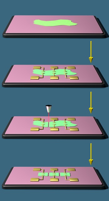
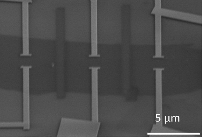
Rice University researchers fabricated a three-pixel, CIS-based optoelectronic sensor array to test the two-dimensional compound’s ability to capture image information. They started with few-layer exfoliated CIS on a silicon substrate, fabricated three pairs of titanium/gold electrodes on top of the CIS and cut the CIS into three sections with a focused ion beam. (Credit: Ajayan Group/Rice University)
In the experiments for the newly reported study, Lei and colleagues grew synthetic CIS crystals, pulled single-layer sheets from the crystals and then tested the ability of the layers to capture light. He said the layer is about two nanometers thick and consists of a nine-atom-thick lattice. The material may also be grown via chemical vapor deposition to a size limited only by the size of the furnace, Lei said.
Because it’s flexible, CIS could also be curved to match the focal surface of an imaging lens system. He said this would allow for the real-time correction of aberrations and significantly simplify the entire optical system.
Co-authors of the paper are Rice graduate students Fangfang Wen and Yongji Gong; postdoctoral researchers Bo Li, Pei Dong, Anthony George and Liehui Ge; undergraduates Qizhong Wang, James Bellah and Yihan Huang; complimentary appointee Yongmin He of Lanzhou University, China; Jun Lou, an associate professor of materials science and nanoengineering, and Naomi Halas, the Stanley C. Moore Professor of Electrical and Computer Engineering and a professor of chemistry, biomedical engineering, physics and astronomy and of materials science and nanoengineering. Ajayan is Rice’s Benjamin M. and Mary Greenwood Anderson Professor in Engineering, professor of materials science and nanoengineering and of chemistry and chair of the Department of Materials Science and NanoEngineering.
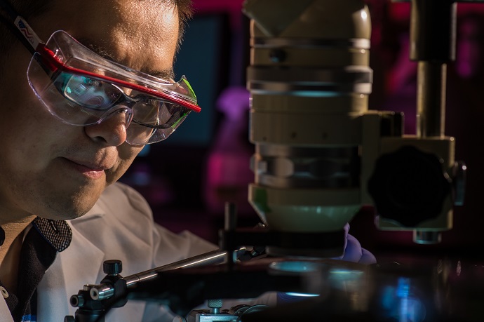
Rice University graduate student Sidong Lei synthesized a two-dimensional material called CIS that shows promise for the development of atomically thin imaging devices. (Credit: Jeff Fitlow/Rice University)

Rice University graduate student Sidong Lei displays a three-pixel prototype made with atomically thin layers of CIS. The new material developed at Rice shows promise for two-dimensional electronics. (Credit: Jeff Fitlow/Rice University)
The research was supported by the Army Research Office Multidisciplinary University Research Initiative, the Function Accelerated nanoMaterial Engineering Division of the Semiconductor Technology Advanced Research Network, the Microelectronics Advanced Research Association, the Defense Advanced Research Projects Agency, the Netherlands Organization for Scientific Research, the Robert A. Welch Foundation, the National Security Science and Engineering Faculty Fellowship and the Office of Naval Research.
Read the abstract at http://pubs.acs.org/doi/abs/10.1021/nl503505f