San Diego, Calif., July 23, 2018 -- Using advanced fabrication techniques, engineers at the University of California San Diego have built a nanosized device out of silver crystals that can generate light by efficiently “tunneling” electrons through a tiny barrier. The work brings plasmonics research a step closer to realizing ultra-compact light sources for high-speed, optical data processing and other on-chip applications.
The work is published July 23 in Nature Photonics.
The device emits light by a quantum mechanical phenomenon known as inelastic electron tunneling. In this process, electrons move through a solid barrier that they cannot classically cross. And while crossing, the electrons lose some of their energy, creating either photons or phonons in the process.
Plasmonics researchers have been interested in using inelastic electron tunneling to create extremely small light sources with large modulation bandwidth. However, because only a tiny fraction of electrons can tunnel inelastically, the efficiency of light emission is typically low—on the order of a few hundredths of a percent, at most.
UC San Diego engineers created a device that bumps that efficiency up to approximately two percent. While this is not yet high enough for practical use, it is the first step to a new type of light source, said Zhaowei Liu, a professor of electrical and computer engineering at the UC San Diego Jacobs School of Engineering.
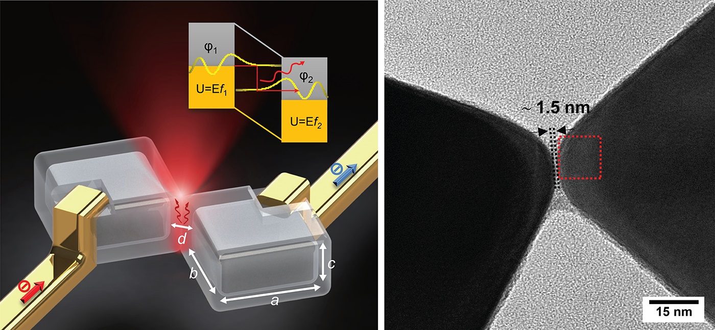
Left: schematics of the tunnel junction formed by two edge-to-edge silver single crystal cuboids with an insulating barrier of polyvinylpyrrolidone (PVP). The top inset shows that photons are generated through inelastic electron tunneling. The device performance can be engineered by tuning the size of the cuboids (a, b, c), the gap size (d), and the curvature of silver cuboid edges. Right: TEM image of the tunnel junction, where the gap is around 1.5 nm. Image courtesy of Haoliang Qian/Nature Photonics
“We’re exploring a new way to generate light,” said Liu.
Liu’s team designed the new light emitting device using computational methods and numerical simulations. Researchers in the lab of Andrea Tao, a professor of nanoengineering at the UC San Diego Jacobs School of Engineering, then constructed the device using advanced solution-based chemistry techniques.
The device is a tiny bow-tie-shaped plasmonic nanostructure consisting of two cuboid, single crystals of silver joined at one corner. Connecting the corners is a 1.5-nanometer-wide barrier of insulator made of a polymer called polyvinylpyrrolidone (PVP).
This tiny metal-insulator-metal (silver-PVP-silver) junction is where the action occurs. Electrodes connected to the nanocrystals allow voltage to be applied to the device. As electrons tunnel from a corner of a silver nanocrystal through the tiny PVP barrier, they transfer energy to surface plasmon polaritons—electromagnetic waves that travel along the metal-insulator interface—which then convert that energy to photons.
But what makes this particular junction more efficient at tunneling electrons inelastically is its geometry and extremely tiny size. By joining two silver single crystals together at their corners with a tiny barrier of insulator in between, researchers essentially created a high quality optical antenna with a high local density of optical states, resulting in more efficient conversion of electronic energy to light.
Metal-insulator-metal junctions have had such low light emission efficiency in the past because they were constructed by joining metal crystals along an entire face, rather than a corner, explained Liu. Giving electrons a high quality optical antenna with a much smaller gap to tunnel through allows efficient light emission, and this kind of structure has been difficult to fabricate with nanolithography methods used in the past, he said.
“Using chemistry, we can build these precise nanosized junctions that allow more efficient light emission,” said Tao. “The fabrication techniques we use give us atomic level control of our materials—we can dictate the size and shape of crystals in solution based on the reagents we use, and we can create structures that have atomically flat faces and extremely sharp corners.”
With additional work, the team aims to further boost efficiency another order of magnitude higher. They are exploring different geometries and materials for future studies.
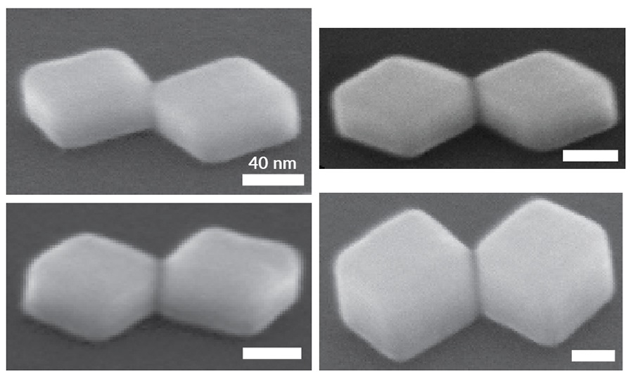
SEM images of silver nanocrystal-based tunnel junctions grown with different dimensions. Image courtesy of Haoliang Qian/Nature Photonics
###
Paper title: “Efficient light generation from enhanced inelastic electron tunneling.” Co-authors include joint co-first authors Haoliang Qian and Su-Wen Hsu; Kargal Gurunatha, Conor T. Riley, Jie Zhao and Dylan Lu.
This work is supported by the Defense Advanced Research Projects Agency (DARPA) Microsystems Technology Office (W911NF-16-2-0156).