11 October 2017
The research of light-matter interactions with nanostructures has become essential in the field of photonics. In such interactions, plasmons play a major role because they are capable of concentrating optical fields down to nanometer-sized regions and enhancing the intensity of incident light by several orders of magnitude.
High-quality graphene plasmons offer the advantages of being electrically, magnetically, and optically tunable, but these outstanding properties are only sensitive to the mid-infrared range. Such properties become very week when trying to use light interactions to generate graphene plasmons in the visible regime.
In a recent study published in ACS Photonics, selected as Editor’s choice by this journal and highlighted in Nature Nanotechnology Research Highlights, ICFO researchers Sandra de Vega and ICREA Prof. at ICFO F. Javier García de Abajo from the Nanophotonics Theory research group at ICFO, have proposed a new theoretical methodology to generate visible plasmons in graphene not from light but from tunnelling electrons.
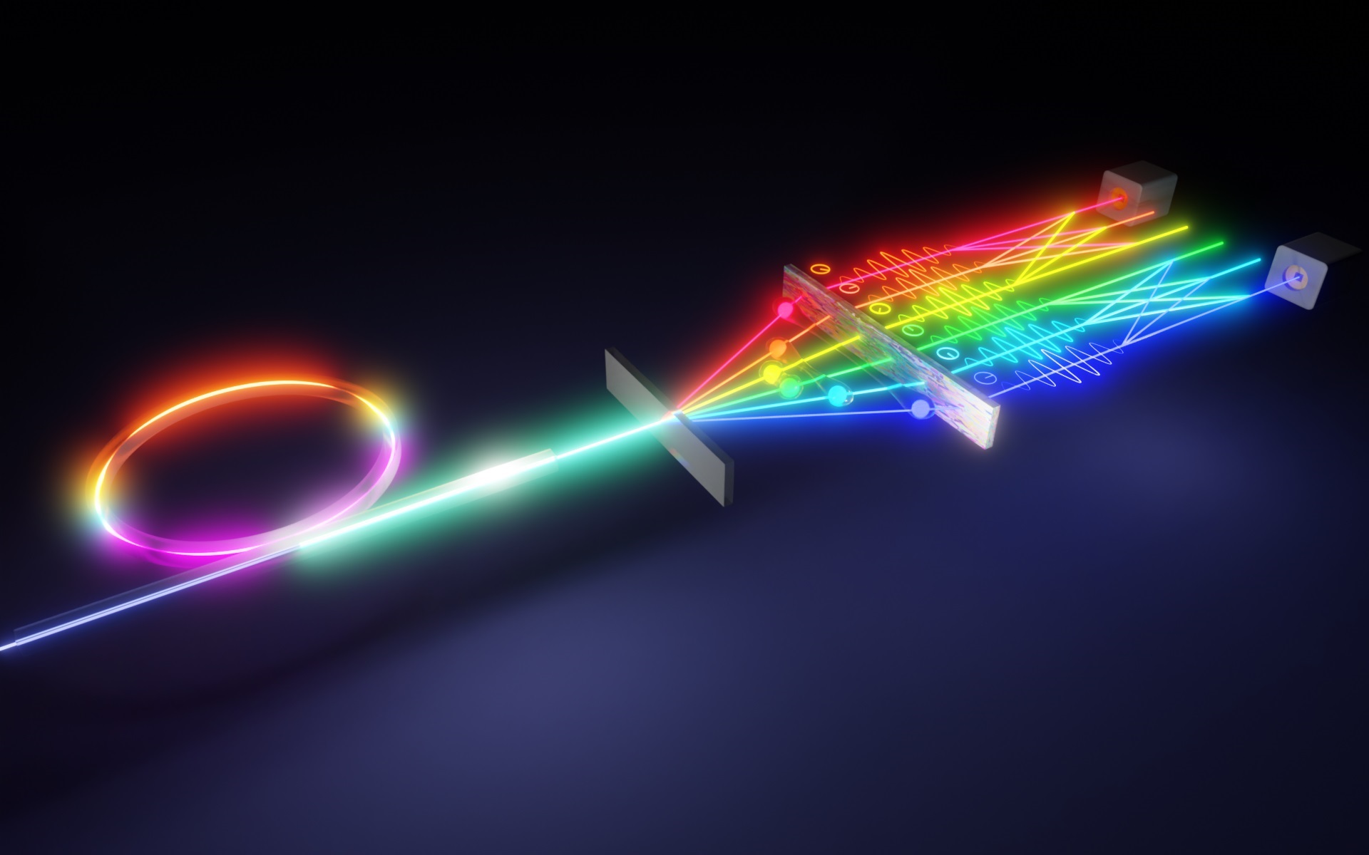
Through theoretical simulations, the team of researchers was able to show that graphene plasmons can be efficiently excited via electron tunnelling in a sandwich structure formed by two graphene monolayers separated by a few atomic layers of hexagonal boron nitride (hBN). In their study, they have found a voltage window in which the tunnelling electrons lose energy through the excitation of a propagating optical plasmon rather than dissipate through coupling with the hBN phonons (low bias) or electron–electron interactions (high bias).
Devices that generate plasmons without the use of light can also be used as sensors, where a change in the graphene plasmon properties is translated into a voltage readout. The short wavelength of graphene plasmons relative to the light wavelength makes them attractive for applications in optoelectronics and sensing.
Visible graphene plasmons from electrons
ICFO researchers propose a method to generate graphene visible plasmons from electron tunnelling.
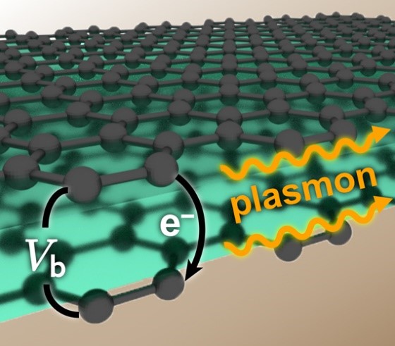
Schematic illustration representing the electron tunneling and plasmon generation in a double-layer graphene structure