16-MAR-2017
Microprocessors play a pivotal role in computers and have steadily increased the speed of information processing over the past several decades. However, due to technical limitations such as heat generation due to integration, the processing speed of semiconductors has remained at several gigahertz (GHz) for the past decade. As a current alternative to this, many microprocessors are used in parallel, but the electrical connection between the processors is slow, creating a bottleneck for data transfer. To solve this problem, many studies have been conducted to merge processors by using optical signals which are several hundred times faster than electrical signals.
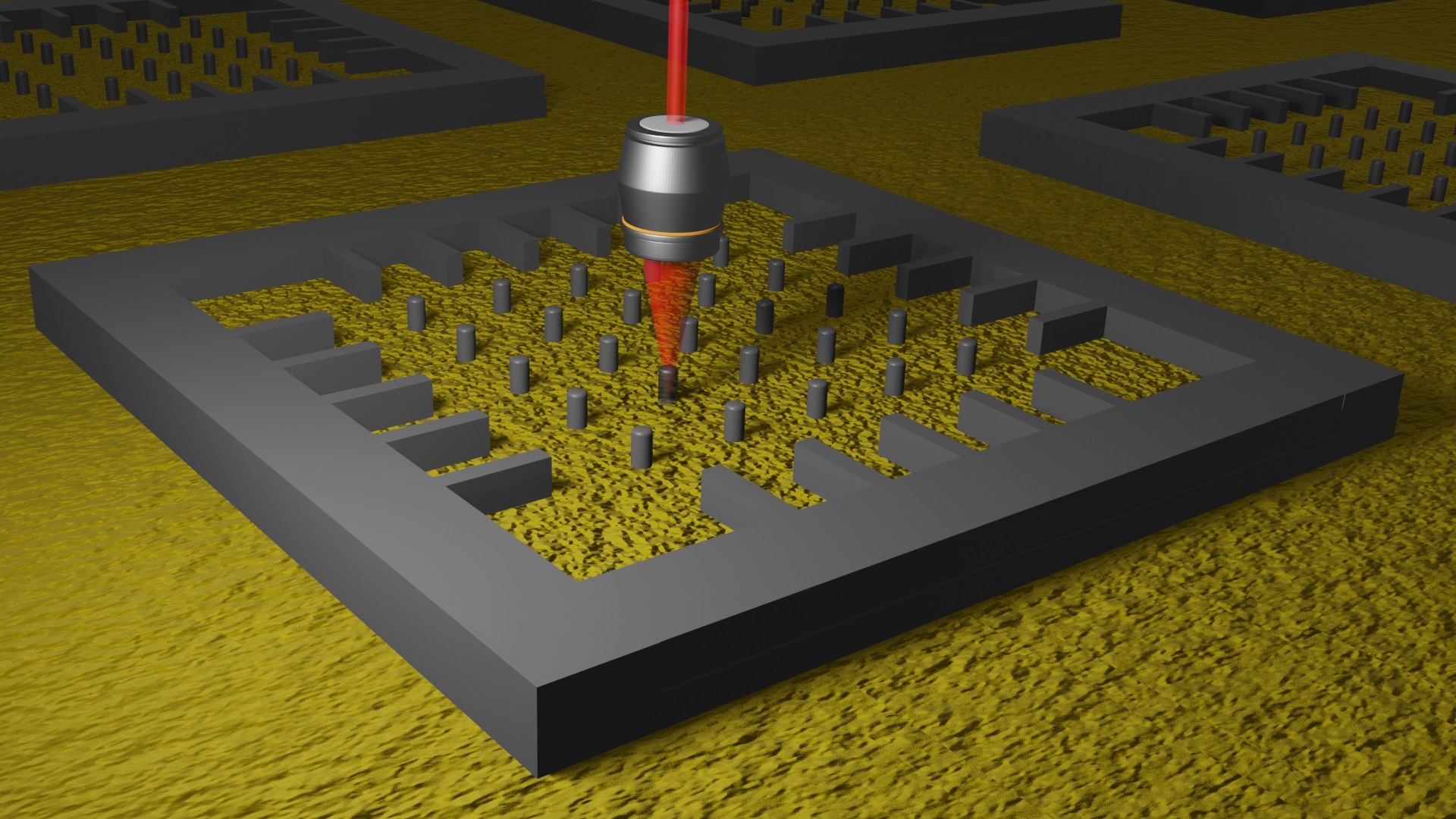
CHOI Wonshik, Associate Director of the CMSD, lead the research team that created an innovative device. The team discarded with the conventional method of periodically arranging the nano antennas. Instead, they devised disordered arrangement of the antennas to minimize redundancy between the antennas and enabled each antenna to function independently. As a result, the device can provide 40 times wider bandwidth than existing antennas periodically arranged. "We are proposing a new way to connect nanoscale microprocessors to ultra-high-speed optical communications," commented Dr. Choi. The research will appear in the March edition of Nature Communications.
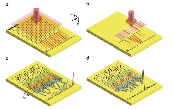
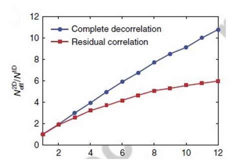
The team used surface plasmons to mediate optoelectronic signaling. At nano antennas, optical signals are converted to surface plasmons, which then propagate through metal surface as electric signals. The researchers randomly arranged the nano antennas, and the surface plasmons generated at each antenna underwent multiple scattering to minimize redundancy between the antennas. In this way, each of the antennas can be used independently, resulting in a substantial increase in the effective number of antennas to more than 40 times. An increase in the number of antennas means an increase in the number of multiple input channels in the MIMO communication, which leads to an increase in the information transmission bandwidth.
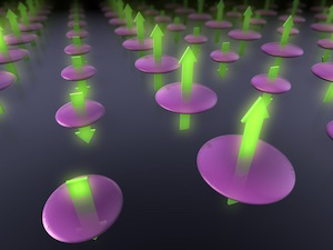
Expected enhancement factor for channel number.
CREDIT: IBS
To exploit the benefit of disordered arrangement of antennas, the team had to resolve an innate problem. Random multiple scattering by disorderly arranged nano antennas is unpredictable, and cannot be used for information transfer without special measure. The researchers analyzed the patterns of multiple-scattered surface plasmons for various optical inputs and found a particular optical input signal that could send the desired signal to a particular microprocessor. The spatial light modulator was used to generate the identified optical input signal, and the surface plasmon could be controlled freely. "Using this," offered Doctor Choi. "We proved that we can transmit signals to six different microprocessors at the same time and proved that optical images are converted into plasmons."
Neil Mannix
RELATED JOURNAL ARTICLE