ST. FLORIAN, Austria and ZURICH, Switzerland, October 9, 2017—EV Group (EVG), a leading supplier of wafer bonding and lithography equipment for the MEMS, nanotechnology and semiconductor markets, and SwissLitho AG, a manufacturer of novel nanolithography tools, today announced a joint solution to enable the production of 3D structures down to the single-nanometer scale. Initially demonstrated within the “Single Nanometer Manufacturing for Beyond CMOS Devices (SNM)” project funded by the Seventh Framework Program of the European Union, the joint solution involves SwissLitho’s novel NanoFrazor thermal scanning probe lithography system to produce master templates with 3D structures for nanoimprint lithography (NIL), and EVG’s HERCULES® NIL system with SmartNIL® technology to replicate those structures at high throughput.
Target Applications
EVG and SwissLitho will initially target the joint solution for developing diffractive optical elements and other related optical components that support photonics, data communications, augmented/virtual reality (AR/VR) and other applications, with the potential to expand into biotechnology, nanofluidics and other nanotechnology applications.
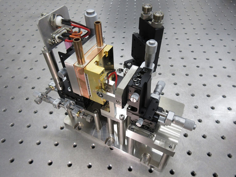
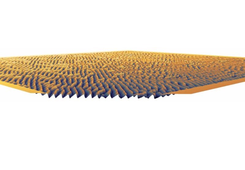
As part of the joint solution, SwissLitho’s NanoFrazor system will be used to create imprint masters. Compared to conventional approaches, including electron beam (e-beam) and grayscale lithography, the novel technology has the unique ability to print 3D structures with unsurpassed accuracy. EVG’s HERCULES NIL system will then be used to create working templates for production use, cost-effectively and at high throughput, using the company’s proprietary large-area nanoimprint SmartNIL technology.
Dr. Thomas Glinsner, corporate technology director at EV Group, noted, “SwissLitho’s NanoFrazor solution is highly complementary to EVG’s SmartNIL technology. Together we can offer a complete NIL solution for photonics and other applications involving 3D structure patterning, providing significant opportunity for both companies to expand our customer base and market reach. Our NILPhotonics® Competence Center will be the first point of contact for customers interested in this joint solution, where we will be able to offer feasibility studies, demonstrations and pilot-line production.”
A Closer Look at the Technologies
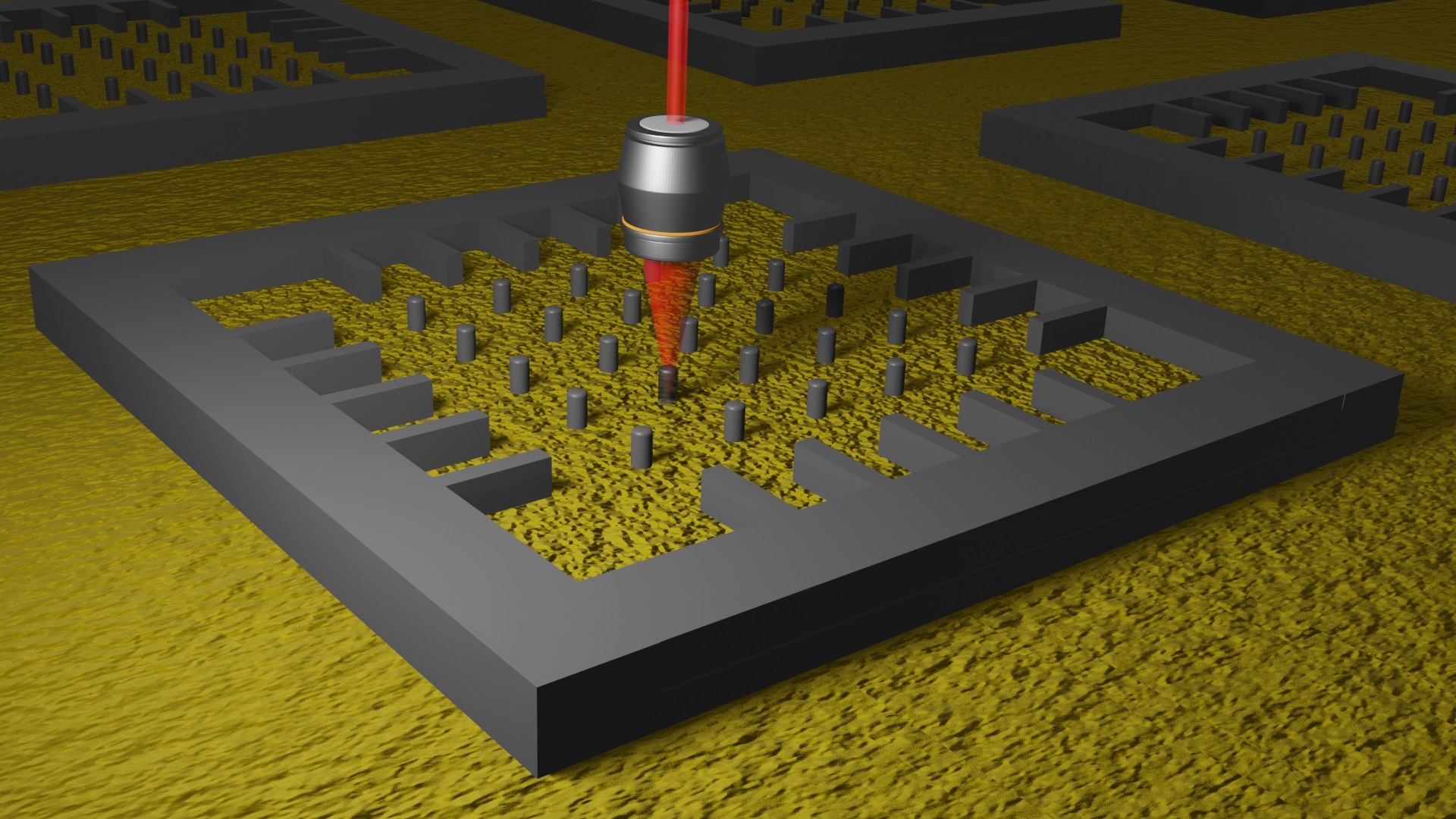
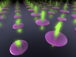
Thermal scanning probe lithography, the technology behind the NanoFrazor, was invented at IBM Research in Zurich and acquired by SwissLitho AG. This maskless, direct-write lithography approach involves spin-coating a unique, thermally sensitive resist onto the sample surface before patterning. A heated ultra-sharp tip is then used to decompose and evaporate the resist locally while simultaneously inspecting the written nanostructures. The resulting arbitrary resist pattern can then be transferred into almost any other material using lift-off, etching, plating, molding or other methodologies.
“We developed our NanoFrazor line to provide a high-performance, affordable alternative and extension to costly e-beam lithography systems,” said Dr. Felix Holzner, SwissLitho CEO. “The technology allows manufacturing of the master with many ‘levels’ in a single step. In particular, 3D structures with single nanometer accuracy can be produced more easily and with greater fidelity compared to traditional e-beam or grayscale lithography methods. We look forward to working with customers to combine our technology with EVG’s successful SmartNIL process at their NILPhotonics Competence Center in Austria.”
The HERCULES NIL combines EVG’s extensive expertise in NIL, resist processing and high-volume manufacturing solutions into a single integrated system that offers throughput of up to 40 wph for 200-mm wafers. The system’s configurable, modular platform accommodates a variety of imprint materials and structure sizes—giving customers greater flexibility in addressing their manufacturing needs. In addition, its ability to fabricate multiple-use soft stamps helps extend the lifetime of master imprint templates.
More information about EVG’s HERCULES NIL UV-NIL track system can be found at: https://www.evgroup.com/en/products/lithography/nanoimprint_systems/uv_nil/hercules_nil/
More information about SwissLitho’s NanoFrazor technology can be found at: https://swisslitho.com/nanofrazor-working-principle/