19 January 2015
by Sam Wong
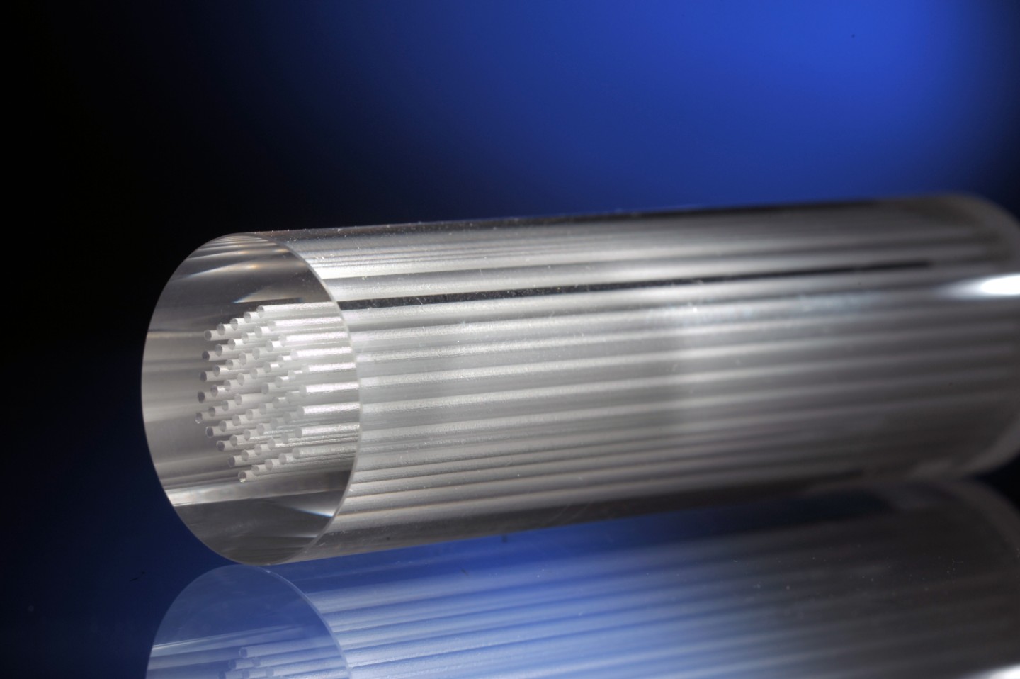
Threatened with extinction by biros and computers, the nib pen could be set to make an unexpected comeback in the field of nanotechnology.
Scientists at Imperial College London have developed a way to manipulate the optical properties of polymers on a tiny scale by drawing patterns with a solvent “ink”, allowing much more precise control over how these materials interact with light.
The technique marks a new approach to creating “metamaterials” – materials with complex internal structures on scales smaller than the wavelength of the light they interact with, resulting in unusual effects.
It could have applications in all kinds of devices that emit, detect and control light, such as LEDs and lasers, photodiodes, and routers and couplers.
The research, which was funded by the Engineering and Physical Sciences Research Council, is published in Nature Communications.
Polymers – the main constituent of plastics – are made of many small molecular repeat units linked together to form chains. Some polymers, referred to as conjugated polymers or polymer semiconductors, are functional optoelectronic materials, meaning for example that they can absorb and emit light.
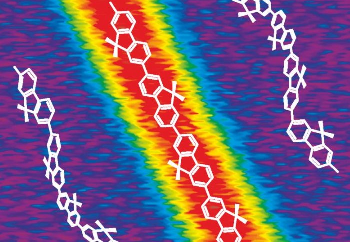
The researchers used a tiny pen to draw patterns on a thin film of polymer semiconductor with a solvent. The solvent changes the shape of a selection of chain segments from a disordered state, like cooked spaghetti, to ordered rigid strands, like uncooked spaghetti. Similar naturally occurring changes in certain biological polymers – specifically proteins – can lead to undesirable disease states but here the changes are deliberately induced and beneficial.
This change in the polymer physical structure alters the way the material interacts with light, changing its refractive index - the amount that light is bent upon entering the material - as well as the colour of light it emits.
The new nib pen (or more commonly termed dip-pen) approach allows scientists to alter these properties on a much smaller scale than they could before, over distances shorter than the wavelength of light. The researchers expect this will make it possible to build a variety of novel structures leading to new and more efficient devices.
One example might be to make tiny LEDs that emit light in one direction only, rather than across a broad range of angles, thereby offering the prospect of compact light source arrays for medical diagnostic applications.
Professor Donal Bradley, Director of the Centre for Plastic Electronicsat Imperial College London, who led the research, said: “Usually we use lenses or mirrors to change the direction of light. This method lets us manipulate a light source itself to tightly control the direction of light that it emits. The material adopts the desired structure naturally - it just requires a little encouragement to do so.”
Aleksandr Perevedentsev, a PhD student who worked on the study, said: “Among other things, this technique essentially allows us to write optical fibers into a thin polymer film, and thus make components that are easy to integrate into devices. It’s very new at the moment, but opens up a lot of possibilities for useful applications. In the process of developing this technique we’ve also began to unravel fundamental questions, such as: can we, in principle, modify the physical structure of a single polymer chain or is an ensemble of chains required for stable structuring? The answer affects the resolution limit of our dip-pen patterning approach and pushes our understanding of these materials beyond the current limits.”
Dr Paul Stavrinou, who led the underpinning theoretical and modeling activity, added: “The ability to pattern at sub-wavelength scales now allows us to manipulate, within the material, the spatial distribution of electromagnetic energy at this length scale. That we achieve this with help from the material itself is the key to achieving more complex photonic patterns.”
Reference: Aleksandr Perevedentsev et al. ‘Dip-pen patterning of poly(9,9-dioctylfluorene) chain-conformation-based nano-photonic elements.’ Nature Communications, 2015. doi:10.1038/ncomms6977