April 16, 2014
The Nanophotonics Group of the Laser Zentrum Hannover e.V. (LZH) has developed a method to print nanoparticles made of different materials with controlled, reproducible sizes and to precisely deposit these particles on a receiver substrate. As a result, for the first time, the scientists succeeded in generating and positioning perfectly round silicon nanoparticles with a diameter of 165 nm. This method was presented in the March 4th issue of Nature Communications.
For the first time, scientists at the LZH were able to fabricate perfectly round silicon nanoparticles with a diameter of 165 nm and to arrange them in ordered structures. This was achieved with their newly developed method that was published in the March 4th issue of Nature Communications. This novel method uses ultrashort laser pulses to print nanoparticles with sizes in the two to three digit nanometer range made of different materials, such as metals, semiconductors and dielectrics. Afterwards, these nanoparticles can be precisely deposited on a receiver substrate.
Nanoparticles exhibit the unique optical property to scatter only light of a particular wavelength. Irradiated with white light and depending on their size, shape and on the interaction with their environment, they appear in a certain color. Therefore, they can be used for various applications in medicine and sensor technology.
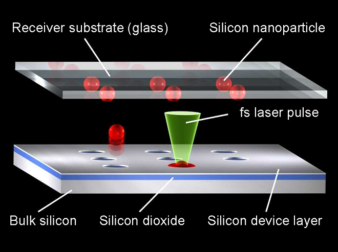
Particle formation through surface tension
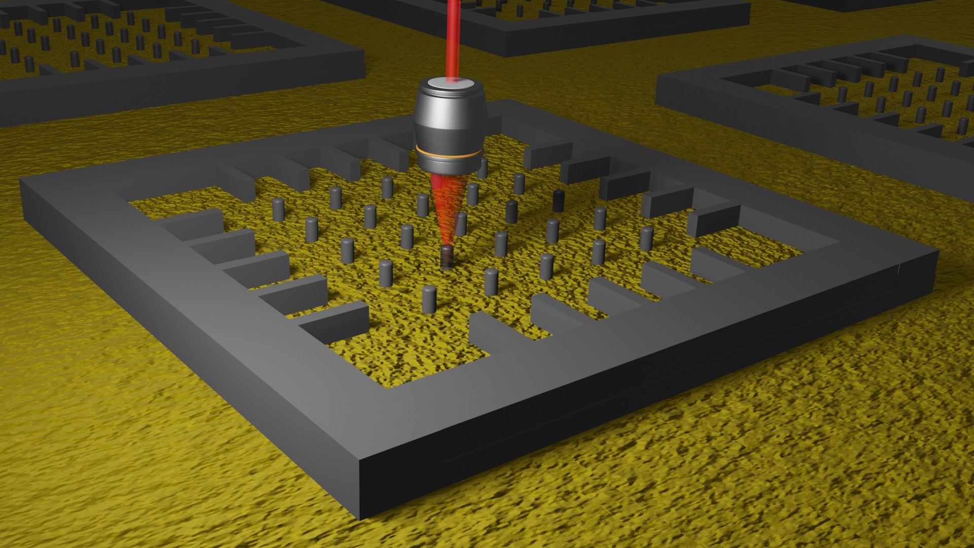
The starting point for the fabrication process is a thin layer of the material of which the nanoparticles shall be made. This layer is irradiated and molten using a single ultrashort laser pulse. Owing to the surface tension of the molten material, a nanosphere is formed which moves up and is finally captured by the receiver substrate. The position of the particles on the receiver material can be controlled very precisely.
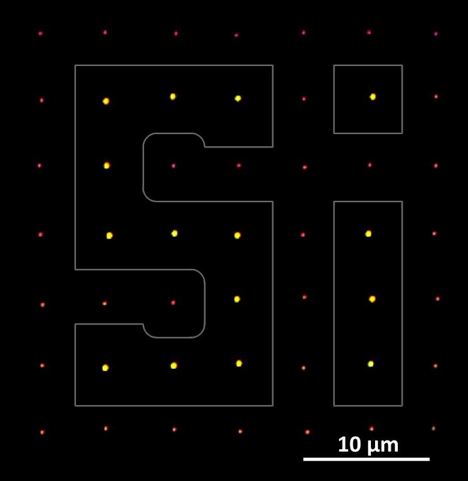
Caption figure 2: Laser-printed silicon nanoparticles in amorphous (red) and crystalline phase (yellow).
Accurate and controllable
„This novel method is the first that allows for both fabricating and precisely depositing nanoparticles of a certain size”, explains Prof. Dr. Boris Chichkov, head of the Nanotechnology Department. “In this respect, our method is far superior to chemical processes which can produce large quantities of nanoparticles but not place them at the desired position.” With this method, two- or three-dimensionally arranged particle structures, such as nanoantennas, nanolasers and metamaterials, can be generated.
From the amorphous to the crystalline phase with the second pulse
The fabrication of silicon nanoparticles of a certain size is particularly interesting because of their special optical properties: They mainly scatter the visible light strongly, and besides the electrical field they also react to the magnetic field component. Other materials, however, almost exclusively interact with the electrical field only. According to the Mie theory, the magnetic light is scattered here, too. After printing, the fabricated silicon particles are in amorphous phase and can be transformed into the crystalline phase with a second laser pulse.
„The results have already lead to the emergence of silicon nanophotonics as a new research field of worldwide interest”, says Chichkov. "Therefore, the new method will certainly find many new applications.
The investigations were carried out within the scope of the SPP 1391 “Ultrafast Nanooptics” priority program and the collaborative research center “Transregio 123 – Planar Optronic Systems” (PlanOS). Both programs are funded by the German Research Foundation (DFG).
The article was published in Nature Communications | 5:3402 | DOI: 10.1038/ncomms4402